Friday 11 January 2013

VLSI - An Introduction


http://www.kokanastha.com/career_guide/introduction_VLSI.html

VLSI - An Introduction

What is VLSI?
VLSI stands for "Very Large Scale Integration". This is the field which involves packing more and more logic devices into smaller and smaller areas.Thanks to VLSI, circuits that would have taken boardfuls of space can now be put into a small space few millimeters across! This has opened up a big opportunity to do things that were not possible before. VLSI circuits are everywhere ... your computer, your car, your brand new state-of-the-art digital camera, the cell-phones, and what have you. All this involves a lot of expertise on many fronts within the same field, which we will look at in later sections.

VLSI has been around for a long time, there is nothing new about it ... but as a side effect of advances in the world of computers, there has been a dramatic proliferation of tools that can be used to design VLSI circuits. Alongside, obeying Moore's law, the capability of an IC has increased exponentially over the years, in terms of computation power, utilisation of available area, yield. The combined effect of these two advances is that people can now put diverse functionality into the IC's, opening up new frontiers. Examples are embedded systems, where intelligent devices are put inside everyday objects, and ubiquitous computing where small computing devices proliferate to such an extent that even the shoes you wear may actually do something useful like monitoring your heartbeats! These two fields are kinda related, and getting into their description can easily lead to another article.
DEALING WITH VLSI CIRCUITS


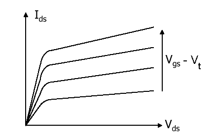
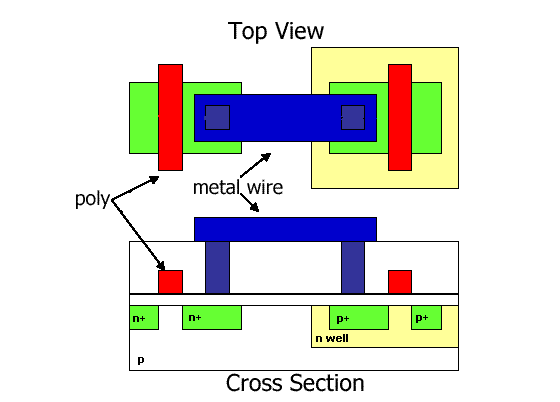
Digital VLSI circuits are predominantly CMOS based. The way normal blocks like latches and gates are implemented is different from what students have seen so far, but the behaviour remains the same. All the miniaturisation involves new things to consider. A lot of thought has to go into actual implementations as well as design. Let us look at some of the factors involved ...

1. Circuit Delays. Large complicated circuits running at very high frequencies have one big problem to tackle - the problem of delays in propagation of signals through gates and wires ... even for areas a few micrometers across! The operation speed is so large that as the delays add up, they can actually become comparable to the clock speeds.

2. Power. Another effect of high operation frequencies is increased consumption of power. This has two-fold effect - devices consume batteries faster, and heat dissipation increases. Coupled with the fact that surface areas have decreased, heat poses a major threat to the stability of the circuit itself.

3. Layout. Laying out the circuit components is task common to all branches of electronics. Whats so special in our case is that there are many possible ways to do this; there can be multiple layers of different materials on the same silicon, there can be different arrangements of the smaller parts for the same component and so on.


The power dissipation and speed in a circuit present a trade-off; if we try to optimise on one, the other is affected. The choice between the two is determined by the way we chose the layout the circuit components. Layout can also affect the fabrication of VLSI chips, making it either easy or difficult to implement the components on the silicon.
THE VLSI DESIGN PROCESS

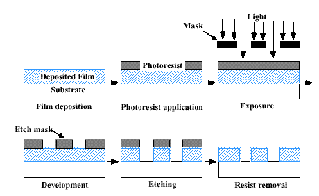
A typical digital design flow is as follows:

Specification
Architecture
RTL Coding
RTL Verification
Synthesis
Backend
Tape Out to Foundry to get end product….a wafer with repeated number of identical Ics.

All modern digital designs start with a designer writing a hardware description of the IC (using HDL or Hardware Description Language) in Verilog/VHDL. A Verilog or VHDL program essentially describes the hardware (logic gates, Flip-Flops, counters etc) and the interconnect of the circuit blocks and the functionality. Various CAD tools are available to synthesize a circuit based on the HDL. The most widely used synthesis tools come from two CAD companies. Synposys and Cadence.

Without going into details, we can say that the VHDL, can be called as the "C" of the VLSI industry. VHDL stands for "VHSIC Hardware Definition Language", where VHSIC stands for "Very High Speed Integrated Circuit". This languages is used to design the circuits at a high-level, in two ways. It can either be a behavioural description, which describes what the circuit is supposed to do, or a structural description, which describes what the circuit is made of. There are other languages for describing circuits, such as Verilog, which work in a similar fashion.

Both forms of description are then used to generate a very low-level description that actually spells out how all this is to be fabricated on the silicon chips. This will result in the manufacture of the intended IC.


A typical analog design flow is as follows:

In case of analog design, the flow changes somewhat.
Specifications
Architecture
Circuit Design
SPICE Simulation
Layout
Parametric Extraction / Back Annotation
Final Design
Tape Out to foundry.

While digital design is highly automated now, very small portion of analog design can be automated. There is a hardware description language called AHDL but is not widely used as it does not accurately give us the behavioral model of the circuit because of the complexity of the effects of parasitic on the analog behavior of the circuit. Many analog chips are what are termed as “flat” or non-hierarchical designs. This is true for small transistor count chips such as an operational amplifier, or a filter or a power management chip. For more complex analog chips such as data converters, the design is done at a transistor level, building up to a cell level, then a block level and then integrated at a chip level. Not many CAD tools are available for analog design even today and thus analog design remains a difficult art. SPICE remains the most useful simulation tool for analog as well as digital design.
MOST OF TODAY’S VLSI DESIGNS ARE CLASSIFIED INTO THREE CATEGORIES:
1. Analog: 
Small transistor count precision circuits such as Amplifiers, Data converters, filters, Phase Locked Loops, Sensors etc.

2. ASICS or Application Specific Integrated Circuits: 
Progress in the fabrication of IC's has enabled us to create fast and powerful circuits in smaller and smaller devices. This also means that we can pack a lot more of functionality into the same area. The biggest application of this ability is found in the design of ASIC's. These are IC's that are created for specific purposes - each device is created to do a particular job, and do it well. The most common application area for this is DSP - signal filters, image compression, etc. To go to extremes, consider the fact that the digital wristwatch normally consists of a single IC doing all the time-keeping jobs as well as extra features like games, calendar, etc.

3. SoC or Systems on a chip: 
These are highly complex mixed signal circuits (digital and analog all on the same chip). A network processor chip or a wireless radio chip is an example of an SoC.

DEVELOPMENTS IN THE FIELD OF VLSI
There are a number of directions a person can take in VLSI, and they are all closely related to each other. Together, these developments are going to make possible the visions of embedded systems and ubiquitous computing.

1. Reconfigurable computing: 
Reconfigurable computing is a very interesting and pretty recent development in microelectronics. It involves fabricating circuits that can be reprogrammed on the fly! And no, we are not talking about microcontrollers running with EEPROM inside. Reconfigurable computing involves specially fabricated devices called FPGA's, that when programmed act just like normal electronic circuits. They are so designed that by changing or "reprogramming" the connections between numerous sub modules, the FPGA's can be made to behave like any circuit we wish.

This fantastic ability to create modifiable circuits again opens up new possibilities in microelectronics. Consider for example, microprocessors which are partly reconfigurable. We know that running complex programs can benefit greatly if support was built into the hardware itself. We could have a microprocessor that could optimise itself for every task that it tackled! Or then consider a system that is too big to implement on hardware that may be limited by cost, or other constraints. If we use a reconfigurable platform, we could design the system so that parts of it are mapped onto the same hardware, at different times. One could think of many such applications, not the least of which is prototyping - using an FPGA to try out a new design before it is actually fabricated. This can drastically reduce development cycles, and also save some money that would have been spent in fabricating prototype IC's

2. Software Engineers taking over hardware design?: 
ASIC's provide the path to creating miniature devices that can do a lot of diverse functions. But with the impending boom in this kind of technology, what we need is a large number of people who can design these IC's. This is where we realise that we cross the threshold between a chip designer and a systems designer at a higher level. Does a person designing a chip really need to know every minute detail of the IC manufacturing process? Can there be tools that allow a designer to simply create design specifications that get translated into hardware specifications?

The solution to this is rather simple - hardware compilers or silicon compilers as they are called. We know by now, that there exist languages like VHDL which can be used to specify the design of a chip. What if we had a compiler that converts a high level language into a VHDL specification? The potential of this technology is tremendous - in simple manner, we can convert all the software programmers into hardware designers!

3. The need for hardware compilers: 
Before we go further let us look at why we need this kind of technology, that can convert high-level languages into hardware definitions. We see a set of needs which actually lead from one to the other in a series.

A. Rapid development cycles.
The traditional method of designing hardware is a long and winding process, going through many stages with special effort spent in design verification at every stage. This means that the time from drawing board to market, is very long. This proves to be rather undesirable in case of large expanding market, with many competitors trying to grab a share. We need alternatives to cut down on this time so that new ideas reach the market faster, where the first person to get in normally gains a large advantage.

B. Large number of designers.
With embedded systems becoming more and more popular, there is a need for a large number of chip designers, who can churn out chips designed for specific applications. Its impractical to think of training so many people in the intricacies of VLSI design.

C. Specialized training.
A person who wishes to design ASIC's will require extensive training in the field of VLSI design. But we cannot possibly expect to find a large number of people who would wish to undergo such training. Also, the process of training these people will itself entail large investments in time and money. This means there has to be system a which can abstract out all the details of VLSI, and which allows the user to think in simple system-level terms.

There are quite a few tools available for using high-level languages in circuit design. But this area has started showing fruits only recently. For example, there is a language called Handel-C, that looks just like good old C. But it has some special extensions that make it usable for defining circuits. A program written in Handel-C, can be represented block-by-block by hardware equivalents. And in doing all this, the compiler takes care of all low-level issues like clock-frequency, layout, etc. The biggest selling point is that the user does not really have to learn anything new, except for the few extensions made to C, so that it may be conveniently used for circuit design.

Another quite different language, that is still under development, is Lava. This is based on an esoteric branch of computer science, called "functional programming". FP itself is pretty old, and is radically different from the normal way we write programs. This is because it assumes parallel execution as a part of its structure - its not based on the normal idea of "sequence of instructions". This parallel nature is something very suitable for hardware since the logic circuits are is inherently parallel in nature. Preliminary studies have shown that Lava can actually create better circuits than VHDL itself, since it affords a high-level view of the system, without losing sight of low-level features.
WHAT SORTS OF JOBS DOES AN ELECTRONICS ENGINEER DO?
As mentioned above, the main job functions in this industry are Design, Product, Test, Applications and Process Engineering. For the sake of clarity, product engineering and test engineering functions are described separately, but it is most efficient to combine these two functions into one engineer because of the interdependency and overlap of skills, tasks and job functions.

1. Design Engineer: 
Takes specifications, defines architecture, does circuit design, runs simulations, supervises layout, tapes out the chip to the foundry, evaluates the prototype once the chip comes back from the fab.

2. Product Engineer: 
Gets involved in the project during the design phase, ensures manufacturability, develops characterization plan, assembly guidelines, develops quality and reliability plan, evaluates the chip with the design engineer, evaluates the chip through characterization, reliability qualification and manufacturing yield point of view (statistical data analysis). He is responsible for production release and is therefore regarded as a team leader on the project. Post production, he is responsible for customer returns, failure analysis, and corrective actions including design changes.

3. Test Engineer: 
Develops test plan for the chip based on specifications and data sheet, creates characterization and production program for the bench test or the ATE (Automatic Test Equipment), designs test board hardware, correlates ATE results with the bench results to validate silicon to compare with simulation results. He works closely with the product engineer to ensure smooth release to production and post release support.

4. Applications Engineer: 
Defines new products from system point of view at the customer’s end, based on marketing input. His mission is to ensure the chip works in the system designed or used by the customers, and complies with appropriate standards (such as Ethernet, SONET, WiFi etc.). He is responsible for all customer technical support, firmware development, evaluation boards, data sheets and all product documentation such as application notes, trade shows, magazine articles, evaluation reports, software drives and so on.

5. Process Engineer: 
This is a highly specialized function which involves new wafer process development, device modeling, and lots of research and development projects. There are no quick rewards on this job! If you are R&D oriented, highly trained in semiconductor device physics area, do not mind wearing bunny suits (the clean room uniforms used in all fabs), willing to experiment, this job is for you.

6. Packaging Engineer: 
This is another highly specialized job function. He develops precision packaging technology, new package designs for the chips, does the characterization of new packages, and does electrical modeling of the new designs.

7. CAD Engineer: 
This is an engineering function that supports the design engineering function. He is responsible for acquiring, maintaining or developing all CAD tools used by a design engineer. Most companies buy commercially available CAD tools for schematic capture, simulation, synthesis, test vector generation, layout, parametric extraction, power estimation, and timing closure; but in several cases, these tools need some type of customization. A CAD engineer needs to be highly skilled in the use of these tools, be able to write software routines to automate as many functions as possible and have a clear understanding of the entire design flow.


 MOS transistor

Voltage on gate controls current that flows between source and drain.
Vt - is the threshold voltage on the gate when drain current begins to flow.
To make the channel conductive Vgs has to be greater than Vt. To make the current flow Vdrain has to be greater than Vsource.
Here is how transistor looks on layout. Drain and source are usually of green or yellow color, gate is red. Transistor is formed when poly (red color) crosses diffusion layer.

W and L are geometry parameters,that actually define the technology. L - defines MAX current, because the larger L the lower R (electrical impedance).
From the other side, large W - means large Capacitance (C=EWL/d).
Capacitance is also increasing with higher integration .
VLSI Technology
PMOS technology based on p-MOS transistors was invented first.
NMOS technology based on n-MOS transistors was used later. n-MOS transistors have better conductance, smaller size and better speed/square performance.
CMOS technology combines n-MOS and p-MOS and has greatest power consumption parameters.
This image illustrates a cross section of CMOS inverter.

VLSI Fabrication
A typical submicron CMOS process uses p-type wafers. A blank 8-inch wafer costs about $100. An IC fabrication process contains a series of masking steps to create layers that define the transistors and metal interconnect. Most layers are formed by the following steps: put layer, protect needed area with photoresist, apply light to transpose, remove photoresist and unprotected layer areas. This photolithografy process is illustrated on the image:

n-well and p-well are formed by ion implantation, when ions of dopped silicon n+ or p+ are forced into wafer area with a great speed. During the implantation the ions can get inside to a depth of a few microns. Further transistor layers are formed by diffusion (high T ion migration). Gates are created from poly (polycristalline silicon). Poly has to have a good conductance. To improve the coductance poly is covered with a silicide (a metallic compaund of silicon). SIO2 is an insulator, it also protects the outer layer from oxidation. Layers of poly and SiO2 can be deposited using chemical vapor deposition (CVD). Metal layers can be deposited using sputtering.All these layers are patterned using masks and photolithografy process.
Power Consumtion
Static power consumption is defined by leakage. Leakage is a junction currents caused by thermally generated carriers. Their value increases exponentially with increasing junction T. For example, 85C (a common junction T) results in increase by a factor of 60 over room T.
Dynamic power consumption depends on a capacitive load:
W= CV2 (charging C to Vdd draws CV2 energy from power supply).
This energy is consumed for every 1 -> 0 and 0 -> 1 transition. Therefor, the higher clock frequency the higher power consumption (~f).
The alternative - is to lower V (power supply voltage).


1 comment:

  1. I admire the way you brought out the general essence of topic on VLSI. Thanks for this blog.Chip level training in hyderabad

    ReplyDelete