Wednesday 9 January 2013

Extrinsic semiconductor


http://www.thebigger.com/physics/conductors-insulators-and-semi-conductors/what-are-extrinsic-semiconductors/


Extrinsic semiconductor


Those semiconductors in which someimpurity atoms are embedded are known as extrinsic semiconductors.
Extrinsic semi conductors are basically of two types:
1. P-type semi conductors
2. N-type semi conductors
N-type Semi conductors: Let’s take an example of the silicon crystal to understand the concept of N-type semi conductor. We have studied the electronic configuration of the silicon atom. It has four electrons in its outermost shell. In N-type semi conductors, the silicon atoms are replaced with the pentavalent atoms like phosphorous, bismuth, antimony etc. So, as a result the four of the electrons of the pentavalent atoms will form the covalent bonds with the silicon atoms and the one electron will revolve around the nucleus of the impurity atoms with less binding energy. These electrons are almost free to move. In other words we can say that these electrons are donated by the impure atoms. So, these are also known as donor atoms. So, the conduction inside the conductor will take place with the help of the negatively charged electrons. Electrons are negatively charged. Due to this negative charge these semiconductors are known as N-type semiconductors.
Each donor atom has denoted an electron from its valence shell. So, as a result due to loss ofthe negative charge these atoms will become positively charged. The single valence electron revolves around the nucleus of the impure atom. Some experiments were performed. It was found that .01eV and .05eV energy is required to make the electron free from the nuclear forces.
When the semi conductors are placed at room temperature then the covalent bond breakage will take place. So, more free electrons will be generated. As a result, same no of holes generation will take place. But as compared to the free electrons the no of holes are comparatively less due to the presence of donor electrons.
We can say that major conduction of n-type semi conductors is due to electrons. So, electrons are known as majority carriers and the holes are known as the minority carriers.
N-type Semi conductors
P-type semi conductors: In a p-type semi conductor doping is done with trivalent atoms .Trivalent atoms are those which have three valence electrons in their valence shell. Some examples of trivalent atoms are Aluminum, boron etc. So, the three valence electrons of the doped impure atoms will form the covalent bonds between silicon atoms. But silicon atoms have four electrons in its valence shell. So, one covalent bond will be improper. So, one more electron is needed for the proper covalent bonding. This need of one electron is fulfilled from any of the bond between two silicon atoms. So, the bond between the silicon and indium atom will be completed. After bond formation the indium will get ionized. As we know that ions are negatively charged. So, indium will also get negative charge. A hole was created when the electron come from silicon-silicon bond to complete the bond between indium and silicon. Now, an electron will move from any one of the covalent bond to fill the empty hole. This will result in a new holes formation. So, in p-type semi conductor the holes movement results in the formation of the current. Holes are positively charged. Hence these conductors are known as p-type semiconductors or acceptor type semi conductors.
When these conductors are placed at room temperature then the covalent bond breakage will take place. In this type of semi conductors the electrons are very less as compared to the holes. So, in p-type semi conductors holes are the majority carriers and electrons are the minority carriers.


Doped (extrinsic) semiconductors

An extrinsic semiconductor is a semiconductor doped by a specific impurity which is able to deeply modify its electrical properties, making it suitable for electronic applications (diodes, transistors, etc.) or optoelectronic applications (light emitters and detectors).

P-type semiconductors

P-type semiconductor is an intrinsic semiconductor (like Si) in which an impurity acting as an acceptor (like e.g. boron B in Si) has been intentionally added. These impurities are called acceptors since once they are inserted in the crystalline lattice, they lack one or several electrons to realize a full bonding with the rest of the crystal.

   
    Figure 5 : schematic representation of a Si crystal doped with boron (B)
Figure 5 : schematic representation of a Si crystal doped with boron (B)  
From figure 5, we see that a p-type semiconductor has a lower electron density n and a higher hole density p than the same intrinsic semiconductor. Electrons are said to be the minority carriers whereas holes are themajority carriers.
For extrinsic semiconductors, the dopant density is always far higher than the intrinsic carrier density : NA>>ni. In the case of a p-type material, the hole density is then close to the dopant density NA. Since the law of mass action is always true, we obtain the following expressions for the carrier densities
The Fermi level for a p-type semiconductor or chemical potential is then :
When the acceptor density is increased, the Fermi level moves closer to the edge of the valence band. If NA=Nv the Fermi level enters the valence band, the semiconductor is then said to be degenerate.
The important points regarding p-type semiconductors are summarized graphically in figure 6.

   
    Figure 6 : P-type semiconductor
Figure 6 : P-type semiconductor  

N-type semiconductors

N-type semiconductor is an intrinsic semiconductor (e.g. silicon Si) in which a donor impurity (e.g. arsenic As in Si, or Si in GaAs) has been intentionally introduced. The impurities are called donor impurities since they have to give an extra electron to the conduction band in order to make all the bonds with neighboring atoms (As is pentavalent while Si is tetravalent).

   
    Figure 7 : Schematic representation of electronic bonds in a Silicon crystal doped with Arsenic As (n doping)
Figure 7 : Schematic representation of electronic bonds in a Silicon crystal doped with Arsenic As (n doping)  
From figure 7, we see that a n-type semiconductor has a higher electron density n and a lower hole density p than the same intrinsic semiconductor. Holes are said to be the minority carriers whereas electrons are themajority carriers.
Like in p-type semiconductors, we can write the following relationships, where ND is the donor density :
The Fermi level for a n-type semiconductor is then :
When the donor density is increased, the Fermi level moves closer to the edge of the conduction band. If ND=Nc the Fermi level enters the conduction band, the semiconductor is then said to be degenerate.
The important points regarding n-type semiconductors are summarized graphically in figure 8.

   
    Figure 8 : N-type semiconductor
Figure 8 : N-type semiconductor  

Intrinsic Semiconductor


Intrinsic semiconductor
n
(Electronics) an almost pure semiconductor to which no impurities have been added and in which the electron and hole densities are equal at thermal equilibrium Also called i-type semiconductor


http://hyperphysics.phy-astr.gsu.edu/hbase/solids/intrin.html


Intrinsic Semiconductor

A silicon crystal is different from an insulator because at any temperature above absolute zero temperature, there is a finite probability that an electron in the lattice will be knocked loose from its position, leaving behind an electron deficiency called a "hole".
If a voltage is applied, then both the electron and the hole can contribute to a small current flow.
The conductivity of a semiconductor can be modeled in terms of the band theory of solids. The band model of a semiconductor suggests that at ordinary temperatures there is a finite possibility that electrons can reach the conduction bandand contribute to electrical conduction.
The term intrinsic here distinguishes between the properties of pure "intrinsic" silicon and the dramatically different properties of doped n-type or p-typesemiconductors.


Electrons and holes


Semiconductor Current

Both electrons and holes contribute to current flow in an intrinsic semiconductor.


Semiconductor Current

The current which will flow in an intrinsic semiconductor consists of bothelectron and hole current. That is, the electrons which have been freed from their lattice positions into the conduction band can move through the material.
In addition, other electrons can hop between lattice positions to fill the vacancies left by the freed electrons. This additional mechanism is called hole conduction because it is as if the holes are migrating across the material in the direction opposite to the free electron movement.
The current flow in an intrinsic semiconductor is influenced by the density of energy states which in turn influences the electron density in the conduction band. This current is highly temperature dependent.

Electrons and Holes

In an intrinsic semiconductor like silicon at temperatures above absolute zero, there will be some electrons which are excited across the band gap into the conduction band and which can produce current. When the electron in pure silicon crosses the gap, it leaves behind an electron vacancy or "hole" in the regular silicon lattice. Under the influence of an external voltage, both the electron and the hole can move across the material. In an n-typesemiconductor, the dopant contributes extra electrons, dramatically increasing the conductivity. In a p-type semiconductor, the dopant produces extra vacancies or holes, which likewise increase the conductivity. It is however the behavior of the p-n junction which is the key to the enormous variety of solid-state electronic devices.

Effective masses of electrons and holes


http://www.optique-ingenieur.org/en/courses/OPI_ang_M05_C02/co/Contenu_03.html

Intrinsic semiconductors

An intrinsic semiconductor is an undoped semiconductor. This means that holes in the valence band are vacancies created by electrons that have been thermally excited to the conduction band, as opposed to doped semiconductors where holes or electrons are supplied by a “foreign” atom acting as an impurity.
In order to better understand the behavior of semiconductors, we need to investigate more deeply what are the electron and hole densities in the conduction and valence bands, respectively. We first need to introduce the notion of energydensity of states N(E). This parameter gives the number of states (per unit volume and per unit energy) between E and E+dE: Nc(E) (respectively, Nv(E)) physically represents the “room” available for electrons (resp. holes) in the conduction band (resp. valence band). For energies that are close to the extrema of these two bands, the density of states has a quadratic dependence with E:
Where  is the normalized Planck constant (h=6.626.10-34Js) and mc(resp. mv) is the average effective mass of the conduction band (resp. of the valence band). For a direct gap semiconductor, mc (resp. mv) is the effective mass of an electron me (resp. a hole mh) in the crystal.
The above-mentioned concept of effective mass allows considering electrons (and holes) inside the crystal as almost free particles, like free quasi-particles. The semiconductor then becomes an electron (and hole) gas, but in which electrons and holes have an effective mass which may be very different of the mass of the particle moving in free space. For example, for GaAs mc/m0=0,066 avec m0=0,911.10-30kg is the free electron mass.
In order to know what is the number of electrons and holes present in each band, the density of states is not the only information that we need. We also have to know the probability for an electron to occupy a level with a given energy E. This probability is given by the Fermi-Dirac distribution function :
Where k=1,38.10-23 JK-1 is the Boltzmann constant, T the temperature and EF the Fermi energy, which is the chemical potential for semiconductors.
The probability for a hole to occupy a level of energy E is simply given by 1-f(E) since a hole is by definition the absence of an electron.
The electron density n [cm-3] in the conduction band is obtained by integrating, over the range of energies accessible by electrons in the band, the number of states that may be occupied by electrons of energy E, weighted by the probability to “find” an electron having this given energy :
Similarly, the hole density p [cm-3] in the valence band writes :
For a semiconductor whose Fermi level EF is located more than 3 kT away from the extrema, the Fermi distribution function can be written under the form of a simple exponential, so that the expressions for the charge carriers densities become :
Where Nc et Nv are called the effective densities of states. They represent the density of “useful” states, at a given temperature T, in their respective energy band.
Let's note that the product of the two densities turns out to be independent on the position of the Fermi level. This is still true even for extrinsic semiconductors (see below). It is known as the law of mass action since it resembles the law of mass action encountered in chemistry (for instance the auto-ionization equilibrium of water is governed by [H+][OH-]=Ke).
Where ni is the density of intrinsic carriers (for Si at 300K, n 1010cm-3).

   
    Figure 3 : Diagram showing the electronic bonds in an intrinsic semiconductor (Si)
Figure 3 : Diagram showing the electronic bonds in an intrinsic semiconductor (Si)  
Figure 3 shows that for an intrinsic semiconductor (without impurities), each electron in the conduction band is associated with a hole in the valence band. We conclude that the electron and hole densities are equal :
By substituting the carrier densities by their respective expressions, this relationship allows defining the Fermi level for an intrinsic semiconductor EFi. Since at room temperature kT is significantly lower than the energy gap, this level is located near the middle of the forbidden band :
In figure 4 are graphically summarized the important points raised above for intrinsic semiconductors.

   
    Figure 4 : Intrinsic semiconductor
Figure 4 : Intrinsic semiconductor  

Types of Semiconductors - Introduction

http://www.brighthubengineering.com/diy-electronics-devices/41694-n-type-and-p-type-semiconductors/


Types of Semiconductors - Introduction


Semiconductors come in a variety of flavours and can be classified as per their majority carriers or dopant types. This article explains all these differences in detail
  • Introduction

    We have covered a lot of ground starting from the basic structure of an atom to the basic concepts of semiconductors and their crystal structure; we will now take a look at the types of semiconductors.
  • Intrinsic Semiconductors

    There are two ways to define an intrinsic semiconductor. In simple words, an intrinsic semiconductor is one which is made up of a very pure semiconductor material. In more technical terminology it can stated that an intrinsic semiconductor is one where the number of holes is equal to the number of electrons in the conduction band.
    The forbidden energy gap in case of such semiconductors is very minute and even the energy available at room temperature is sufficient for the valence electrons to jump across to the conduction band.
    Another characteristic feature of an intrinsic semiconductor is that the Fermi level of such materials lies somewhere in between the valence band and the conduction band. This can be proved mathematically which is beyond the scope of discussion in this article. In case you are not familiar with the term Fermi level, it refers to that level of energy where the probability of finding an electron is 0.5 or half (remember probability is measured on a scale of 0 to 1).

  • Extrinsic Semiconductors

    These are semiconductors in which the pure state of the semiconductor material is deliberately diluted by adding very minute quantities of impurities. To be more specific, the impurities are known as dopants or doping agents. It must be kept in mind that the addition of such impurities is really very minuscule and a typical dopant could have a concentration of the order of 1 part in a hundred million parts or it is equivalent to 0.01 ppm.
    The materials chosen for doping are deliberately chosen in such a manner that either they have 5 electrons in their valence band, or they have just 3 electrons in their valence band. Accordingly such dopants are known as pentavalent or trivalent dopants respectively.
    The type of dopant also gives rise to two types of extrinsic semiconductors namely P-type and N-type semiconductors.
    A pentavalent dopant such as Antimony are known as donor impurities since they donate an extra electron in the crystal structure which is not required for covalent bonding purposes and is readily available to be shifted to the conduction band. This electron does not give rise to a corresponding hole in the valence band because it is already excess, therefore upon doping with such a material, the base material such as Germanium contains more electrons than holes, hence the nomenclature N-type intrinsic semiconductors.
    On the other hand when a trivalent dopant such as Boron is added to Germanium additional or extra holes get formed due to the exactly reverse process of what was described in the upper section. Hence this dopant which is also known as acceptor creates a P-type semiconductor.
    Hence electrons are the majority carriers (of current) in N-type while holes are minority carriers. The reverse is true of P-type semiconductors. Another difference is that whereas the Fermi level of intrinsic semiconductors is somewhere midway between the valence band and the conduction band, it shifts upwards in case of N-type while it drifts downward in case of P-type due to obvious reasons.
    Having learnt about various types of semiconductors, we will now see what happens in case the N-type and P-type semiconductor materials are joined together to form a junction known as the P-N junction and how is it useful for digital electronics.

Semiconductor - Description(Wiki), Working and Properties

http://en.wikipedia.org/wiki/Semiconductor


Semiconductor


semiconductor is a material which has electrical conductivity between that of a conductor such as copper and an insulator such as glass. The conductivity of a semiconductor increases with increasing temperature, the opposite behaviour to a metal.[1] Semiconductors can display a range of useful properties such as passing current more easily in one direction than the other. Because the conductive properties of a semiconductor can be modified by controlled addition of impurities or by the application of electrical fields or light, semiconductors are very useful devices for amplification of signals, switching, and energy conversion. Understanding the properties of semiconductors relies on quantum physics to explain the motions of electrons through a lattice of atoms.
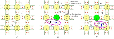
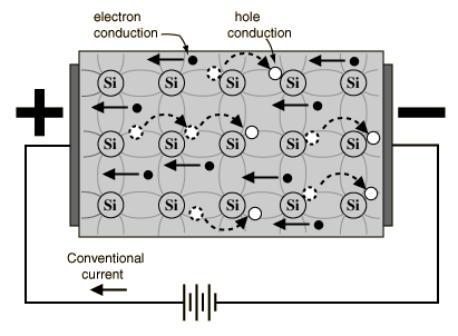
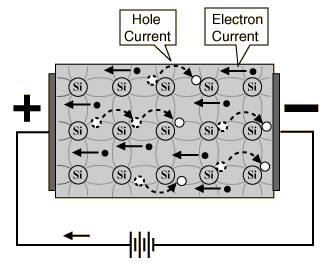
Current conduction in a semiconductor occurs via free electrons and "holes", collectively known as charge carriers. Adding impurity atoms to a semiconducting material, known as "doping", greatly increases the number of charge carriers within it. When a doped semiconductor contains excess holes it is called "p-type", and when it contains excess free electrons it is known as "n-type". The semiconductor material used in devices is doped under highly controlled conditions to precisely control the location and concentration of p- and n-type dopants. A single semiconductor crystal can have multiple p- and n-type regions; the p-n junctions between these regions have many useful electronic properties.
Semiconductors are the foundation of modern electronics, including radio, computers, and telephones. Semiconductor-based electronic components include transistorssolar cells, many kinds of diodes including thelight-emitting diode (LED), the silicon controlled rectifier, photo-diodes, and digital and analog integrated circuits. Increasing understanding of semiconductor materials and fabrication processes has made possible continuing increases in the complexity and speed of semiconductor devices, an effect known as Moore's Law.

Materials

A large number of elements and compounds have semiconducting properties, including:[1]
  • Certain pure elements found in Group IV of the periodic table; the most commercially important of these elements are silicon and germanium.
  • Binary compounds, particularly between elements in Groups III and V, such as gallium arsenide, Groups II and VI, groups IV and VI, and between different group IV elements, e.g. silicon carbide.
  • Certain ternary compounds, oxides and alloys.
  • A number of organic compounds.
An intrinsic semiconductor is made up of one pure element or pure compound. At room temperature, the conductivity of intrinsic semiconductors is relatively low because there are very few charge carriers available. Conductivity is greatly enhanced by a process called doping, in which very small amounts of other elements are added to the intrinsic crystal to create what is called an extrinsic semiconductor.
Most common semiconducting materials are crystalline solids, but amorphous and liquid semiconductors are also known. These include hydrogenated amorphous silicon and mixtures of arsenicselenium and tellurium in a variety of proportions. These compounds share with better known semiconductors the properties of intermediate conductivity and a rapid variation of conductivity with temperature, as well as occasional negative resistance. Such disordered materials lack the rigid crystalline structure of conventional semiconductors such as silicon. They are generally used in thin film structures, which do not require material of higher electronic quality, being relatively insensitive to impurities and radiation damage.

[edit]Energy bands and electrical conduction

Semiconductors are defined by their unique electric conductive behavior. Metals are good conductors because at their Fermi level, there is a large density of energetically available states that each electron can occupy. Electrons can move quite freely between energy levels without a high energy cost. Metal conductivity decreases with temperature increase because thermal vibrations of crystal lattice disrupt the free motion of electrons. Insulators, by contrast, are very poor conductors of electricity because there is a large difference in energies (called a band gap) between electron-occupied energy levels and empty energy levels that allow for electron motion.
Insulator conductivity increases with temperature because heat provides energy to promote electrons across the band gap to the higher electron conduction energy levels (called the conduction band). Semiconductors, on the other hand, have an intermediate level of electric conductivity when compared to metals and insulators. Their band gap is small enough that small increase in temperature promotes sufficient number of electrons (to result in measurable currents) from the lowest energy levels (in the 
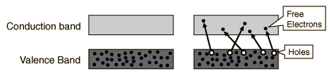
valence band) to the conduction band. This createselectron holes, or unoccupied levels, in the valence band, and very loosely held electrons in the conduction band.[4][5]

A simplified diagram illustrating the energy band levels of an insulator, a semiconductor, and a conductor. Electrons can only exist in certain energy levels.
In the classic crystalline semiconductors, electrons can have energies only within certain bands (ranges). The range of energy runs from the ground state, in which electrons are tightly bound to the atom, up to a level where the electron can escape entirely from the material. Each energy band corresponds to a large number of discrete quantum statesof the electrons. Most of the states with low energy (closer to the nucleus) are occupied, up to a particular band called the valence band.
Semiconductors and insulators are distinguished from metals by the population of electrons in each band. The valence band in any given metal is nearly filled with electrons under usual conditions, and metals have many free electrons with energies in the conduction band. In semiconductors, only a few electrons exist in the conduction band just above the valence band, and an insulator has almost no free electrons.
The ease with which electrons in the semiconductor can be excited from the valence band to the conduction band depends on the band gap. The size of this energy gap (bandgap) determines whether a material is semiconductor or an insulator (nominally this dividing line is roughly 4 eV).
With covalent bonds, an electron moves by hopping to a neighboring bond. The Pauli exclusion principle requires the electron to be lifted into the higher anti-bonding state of that bond. For delocalized states, for example in one dimension – that is in a nanowire, for every energy there is a state with electrons flowing in one direction and another state with the electrons flowing in the other. For a net current to flow, more states for one direction than for the other direction must be occupied. For this to occur, energy is required, as in the semiconductor the next higher states lie above the band gap. Often this is stated as: full bands do not contribute to the electrical conductivity. However, as the temperature of a semiconductor rises above absolute zero, there is more energy in the semiconductor to spend on lattice vibration and on exciting electrons into the conduction band.
Electrons excited to the conduction band also leave behind electron holes, i.e. unoccupied states in the valence band. Both the conduction band electrons and the valence band holes contribute to electrical conductivity. The holes themselves don't move, but a neighboring electron can move to fill the hole, leaving a hole at the place it has just come from, and in this way the holes appear to move, and the holes behave as if they were actual positively charged particles.
One covalent bond between neighboring atoms in the solid is ten times stronger than the binding of the single electron to the atom, so freeing the electron does not imply destruction of the crystal structure.

[edit]Explaining energy bands

The theory of electron energy levels in solids is an application of the principles of quantum mechanics. In principle, the motions of electrons can be predicted by solution of Schrödinger's equation for the potential field of a particular arrangement of atoms in a crystal. Since a general solution is quite difficult, various simplifying assumptions are used to represent the actual system.
A fundamental observation leading to the development of quantum mechanics is that the energy levels of an electron around an atom does not vary continuously, but instead occurs in discrete quantum states called "orbitals", each associated with an amount of energy. Another observation, stated as the Pauli exclusion principle, is that no two electrons can occupy exactly the same quantum state; so, not all the electrons of the atom fall into the lowest state, but occupy increasingly energetic "shells" around the atom.
Putting two atoms together leads to delocalized orbitals across two atoms, yielding a partially covalent bond. Additional quantum states are possible, in this molecular orbital, with different energy levels.
In a crystal, many atoms are adjacent and many energy levels are possible for electrons. Since there are so many (on the order of 1022) atoms in a macroscopic crystal, the resulting energy states available for electrons are very closely spaced. Since the Heisenberg principle limits the precision of any measurement of the combination of an electron's momentum (related to energy) and its position, in a crystal effectively the available energy levels form a continuous band of allowed energy levels.
The mathematical solution of the Schrödinger equation gives two kinds of solutions depending on the energy of the electrons. One type of solution represents an electron moving indefinitely through the crystal as a plane wave; the particular solutions for a periodic regular crystal lattice are called Bloch functions. A second type of solution occurs for energy levels in the so-called "forbidden" gaps between "allowed" states - in this case, the electron cannot travel indefinitely through the crystal with that energy and will either be reflected at the edges of the region, or possibly must pass through the region in a phenomenon called "quantum tunnelling".
For semiconductor materials, one band of "allowed" electron energies is called the "valence band" - these can be thought of electrons bound to a particular atom. A higher-energy band is called the "conduction band", where electrons may travel through the crystal.[6] The energy of an electron may be increased by increasing its temperature or by applying an electric field to it. If a band of allowable energies is completely filled by electrons, it cannot carry any electrical current, because that would require the electron's energy to be increased. Conduction can only occur with partially filled bands.
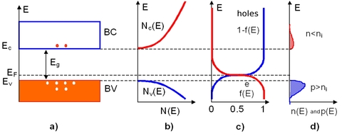
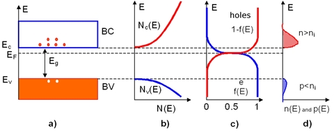
The Fermi energy plays an important role in describing the behavior of doped semiconductors. A substance’s Fermi energy is defined as the highest occupied energy level found in that substance at absolute zero temperature (0 kelvins or -273 °C). At higher temperatures, energy from heat is available to promote electrons into slightly higher energy levels. However, picturing the density of states to be filled to the Fermi energy helps scientists understand different behaviors between insulators, metals, and intrinsic and extrinsic semiconductors. As seen in Figure 1 (below), the Fermi energy of n-type semiconductors is elevated from that of the corresponding un-doped intrinsic semiconductor. This makes the conduction band much more thermally accessible at temperatures above absolute zero.[5]

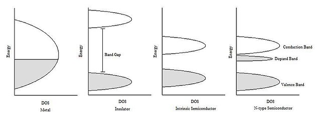
Figure 1: Representative density of states diagrams of metals, insulators, intrinsic and n-doped semiconductors. Shaded areas represent energy levels filled at absolute zero, below the Fermi energy.
The Fermi level is the energy below which there is a 50% chance of finding an occupied energy state. The Fermi level can be calculated from the density of states in the conduction and valence bands. The Fermi level may increase, remain the same or decrease with increasing temperature, depending on the number of states in the conduction and valence bands. Where two regions with different Fermi levels are in contact, charge carriers will flow between the two regions until the Fermi level is aligned across the interface.
At absolute zero temperature the Fermi level can be thought of as the energy up to which available electron states are occupied. At higher temperatures, the Fermi level is the energy at which the probability of a state being occupied has fallen to 0.5.

[edit]Holes: electron absence as a charge carrier

The concept of holes can also be applied to metals, where the Fermi level lies within the conduction band. With most metals the Hall effect indicates electrons are the charge carriers. However, some metals have a mostly filled conduction band. In these, the Hall effect reveals positive charge carriers, which are not the ion-cores, but holes. In the case of a metal, only a small amount of energy is needed for the electrons to find other unoccupied states to move into, and hence for current to flow. Sometimes even in this case it may be said that a hole was left behind, to explain why the electron does not fall back to lower energies: It cannot find a hole. In the end in both materials electron-phonon scattering and defects are the dominant causes for resistance.

Fermi-Dirac distribution. States with energy ε below the Fermi level, here µ, have higher probability n to be occupied, and those above are less likely to be occupied. Smearing of the distribution increases with temperature.
The energy distribution of the electrons determines which of the states are filled and which are empty. This distribution is described by Fermi-Dirac statistics. The distribution is characterized by the temperature of the electrons, and the Fermi level. The dependence of the electron energy distribution on temperature also explains why the conductivity of a semiconductor has a strong temperature dependency, as a semiconductor operating at lower temperatures will have fewer available free electrons and holes able to do the work.

[edit]Energy–momentum dispersion

In the preceding description an important fact is ignored for the sake of simplicity: the dispersionof the energy. The reason that the energies of the states are broadened into a band is that the energy depends on the value of the wave vector, or k-vector, of the electron. The k-vector, in quantum mechanics, is the representation of the momentum of a particle.
The dispersion relationship determines theeffective massm*, of electrons or holes in the semiconductor, according to the formula:
 m^{*} = \hbar^2 \cdot \left[ {{d^2 E(k)} \over {d k^2}} \right]^{-1}.
The effective mass is important as it affects many of the electrical properties of the semiconductor, such as the electron or hole mobility, which in turn influences the diffusivity of the charge carriers and the electrical conductivityof the semiconductor.
Typically the effective mass of electrons and holes are different. This affects the relative performance of p-channeland n-channel IGFETs.[7]
The top of the valence band and the bottom of the conduction band might not occur at that same value of k. Materials with this situation, such as silicon and germanium, are known as indirect bandgap materials. Materials in which the band extrema are aligned in k, for example gallium arsenide, are called direct bandgap semiconductors. Direct gap semiconductors are particularly important in optoelectronics because they are much more efficient as light emitters than indirect gap materials; an electron moving between two bands need not exchange momentum with phonons in the crystal lattice.

[edit]Carrier generation and recombination

When ionizing radiation strikes a semiconductor, it may excite an electron out of its energy level and consequently leave a hole. This process is known as electron–hole pair generation. Electron-hole pairs are constantly generated from thermal energy as well, in the absence of any external energy source.
Electron-hole pairs are also apt to recombine. Conservation of energy demands that these recombination events, in which an electron loses an amount of energy larger than the band gap, be accompanied by the emission of thermal energy (in the form of phonons) or radiation (in the form of photons).
In some states, the generation and recombination of electron–hole pairs are in equipoise. The number of electron-hole pairs in the steady state at a given temperature is determined by quantum statistical mechanics. The precisequantum mechanical mechanisms of generation and recombination are governed by conservation of energy andconservation of momentum.
As the probability that electrons and holes meet together is proportional to the product of their amounts, the product is in steady state nearly constant at a given temperature, providing that there is no significant electric field (which might "flush" carriers of both types, or move them from neighbour regions containing more of them to meet together) or externally driven pair generation. The product is a function of the temperature, as the probability of getting enough thermal energy to produce a pair increases with temperature, being approximately exp(−EG/kT), where k is Boltzmann's constantT is absolute temperature and EG is band gap.
The probability of meeting is increased by carrier traps—impurities or dislocations which can trap an electron or hole and hold it until a pair is completed. Such carrier traps are sometimes purposely added to reduce the time needed to reach the steady state.

[edit]Doping

The conductivity of semiconductors may easily be modified by introducing impurities into their crystal lattice. The process of adding controlled impurities to a semiconductor is known as doping. The amount of impurity, or dopant, added to an intrinsic (pure) semiconductor varies its level of conductivity. Doped semiconductors are referred to asextrinsic. By adding impurity to pure semiconductors, the electrical conductivity may be varied by factors of thousands or millions.
A 1 cm3 specimen of a metal or semiconductor has of the order of 1022 atoms. In a metal, every atom donates at least one free electron for conduction, thus 1 cm3 of metal contains on the order of 1022 free electrons. Whereas a 1 cm3 of sample pure germanium at 20 °C, contains about 4.2×10²² atoms but only 2.5×10¹³ free electrons and 2.5×10¹³ holes. The addition of 0.001% of arsenic (an impurity) donates an extra 1017 free electrons in the same volume and the electrical conductivity is increased by a factor of 10,000.
The materials chosen as suitable dopants depend on the atomic properties of both the dopant and the material to be doped. In general, dopants that produce the desired controlled changes are classified as either electronacceptors or donors. Semiconductors doped with donor impurities are called n-type, while those doped withacceptor impurities are known as p-type. The n and p type designations indicate which charge carrier acts as the material's majority carrier. The opposite carrier is called the minority carrier, which exists due to thermal excitation at a much lower concentration compared to the majority carrier.
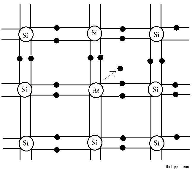
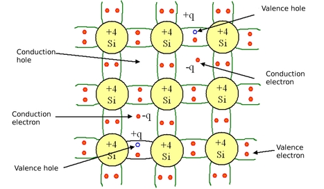
For example, the pure semiconductor silicon has four valence electrons which bond each silicon atom to its neighbors. In silicon, the most common dopants are group III and group V elements. Group III elements all contain three valence electrons, causing them to function as acceptors when used to dope silicon. When an acceptor atom replaces a silicon atom in the crystal, a vacant state ( an electron "hole") is created, which can move around the lattice and functions as a charge carrier. Group V elements have five valence electrons, which allows them to act as a donor; substitution of these atoms for silicon creates an extra free electron. Therefore, a silicon crystal doped with boron creates a p-type semiconductor whereas one doped with phosphorus results in an n-type material.
During manufacture, dopants can be diffused into the semiconductor body by contact with gaseous compounds of the desired element, or ion implantation can be used to accurately position the doped regions.

[edit]Preparation of semiconductor materials

Semiconductors with predictable, reliable electronic properties are necessary for mass production. The level of chemical purity needed is extremely high because the presence of impurities even in very small proportions can have large effects on the properties of the material. A high degree of crystalline perfection is also required, since faults in crystal structure (such as dislocationstwins, and stacking faults) interfere with the semiconducting properties of the material. Crystalline faults are a major cause of defective semiconductor devices. The larger the crystal, the more difficult it is to achieve the necessary perfection. Current mass production processes use crystalingots between 100 mm and 300 mm (4–12 inches) in diameter which are grown as cylinders and sliced intowafers.
Because of the required level of chemical purity and the perfection of the crystal structure which are needed to make semiconductor devices, special methods have been developed to produce the initial semiconductor material. A technique for achieving high purity includes growing the crystal using the Czochralski process. An additional step that can be used to further increase purity is known as zone refining. In zone refining, part of a solid crystal is melted. The impurities tend to concentrate in the melted region, while the desired material recrystalizes leaving the solid material more pure and with fewer crystalline faults.
In manufacturing semiconductor devices involving heterojunctions between different semiconductor materials, thelattice constant, which is the length of the repeating element of the crystal structure, is important for determining the compatibility of materials.

[edit]Organic materials

Organic semiconductors have been of great research interest for use in low cost, ultra thin, and flexible products such as displays and solar cells. While many p-type organic semiconductors have been thoroughly characterized, n-type organic semiconductors have proven hard to obtain. Both types are needed for the diodes and transistors that make desirable devices possible. N-type organic semiconductors were produced of the arylene diimide family that are resistant to thermal and environmental stresses, which is one of the largest challenges in the field.[8]Several other compounds are being explored for n-type organic semiconductors for use in organic field-effect transistors (OFET), such as fullerene (C60) and chemically modified oligothiophenes. Semiconductors are made from these compounds by reduction with electron withdrawing groups or, alternatively, by modifying the surface properties to control electron trapping.[9] Organic thin film transistors (OTFTs) are being explored because their low synthesis temperatures allow them to be deposited on thin plastic substrates without damage, resulting in thin and flexible devices. Same compounds are often considered for use in OFETs and OTFTs.[10]

[edit]Semi-insulators

Some materials are classified as semi-insulators. These have electrical conductivity nearer to that of electrical insulators. Semi-insulators find niche applications in micro-electronics, such as substrates for HEMT. An example of a common semi-insulator is gallium arsenide.[11]


http://electronics.howstuffworks.com/diode3.htm

Working of semiconductors


Semiconductors have had a monumental impact on our society. You find semiconductors at the heart of microprocessor chips as well as transistors. Anything that's computerized or uses radio waves depends on semiconductors.
Today, most semiconductor chips and transistors are created withsilicon. You may have heard expressions like "Silicon Valley" and the "silicon economy," and that's why -- silicon is the heart of any electronic device.
diode is the simplest possible semiconductor device, and is therefore an excellent beginning point if you want to understand how semiconductors work. In this article, you'll learn what a semiconductor is, how doping works and how a diode can be created using semiconductors. But first, let's take a close look at silicon.
Silicon is a very common element -- for example, it is the main element in sand and quartz. If you look "silicon" up in the periodic table, you will find that it sits next to aluminum, below carbon and above germanium.

Silicon sits next to aluminum and below carbon in the periodic table.
Carbon, silicon and germanium (germanium, like silicon, is also a semiconductor) have a unique property in their electron structure -- each has four electrons in its outer orbital. This allows them to form nice crystals. The four electrons form perfect covalent bonds with four neighboring atoms, creating a lattice. In carbon, we know the crystalline form asdiamond. In silicon, the crystalline form is a silvery, metallic-looking substance.

In a silicon lattice, all silicon atoms bond perfectly to four neighbors, leaving no free electrons to conduct electric current. This makes a silicon crystal an insulator rather than a conductor.


Doping Silicon

You can change the behavior of silicon and turn it into a conductor by doping it. In doping, you mix a small amount of an impurity into the silicon crystal.
There are two types of impurities:
  • N-type - In N-type doping,phosphorus or arsenic is added to the silicon in small quantities. Phosphorus and arsenic each have five outer electrons, so they're out of place when they get into the silicon lattice. The fifth electron has nothing to bond to, so it's free to move around. It takes only a very small quantity of the impurity to create enough free electrons to allow an electric current to flow through the silicon. N-type silicon is a good conductor. Electrons have a negative charge, hence the name N-type.
  • P-type - In P-type doping, boron or gallium is the dopant. Boron and gallium each have only three outer electrons. When mixed into the silicon lattice, they form "holes" in the lattice where a silicon electron has nothing to bond to. The absence of an electron creates the effect of a positive charge, hence the name P-type. Holes can conduct current. A hole happily accepts an electron from a neighbor, moving the hole over a space. P-type silicon is a good conductor.
A minute amount of either N-type or P-type doping turns a silicon crystal from a good insulator into a viable (but not great) conductor -- hence the name "semiconductor."
N-type and P-type silicon are not that amazing by themselves; but when you put them together, you get some very interesting behavior at the junction. That's what happens in a diode.
diode is the simplest possible semiconductor device. A diode allows current to flow in one direction but not the other. You may have seen turnstiles at a stadium or a subway station that let people go through in only one direction. A diode is a one-way turnstile for electrons.
When you put N-type and P-type silicon together as shown in this diagram, you get a very interesting phenomenon that gives a diode its unique properties.

Even though N-type silicon by itself is a conductor, and P-type silicon by itself is also a conductor, the combination shown in the diagram does not conduct any electricity. The negative electrons in the N-type silicon get attracted to the positive terminal of thebattery. The positive holes in the P-type silicon get attracted to the negative terminal of the battery. No current flows across the junction because the holes and the electrons are each moving in the wrong direction.
If you flip the battery around, the diode conducts electricity just fine. The free electrons in the N-type silicon are repelled by the negative terminal of the battery. The holes in the P-type silicon are repelled by the positive terminal. At the junction between the N-type and P-type silicon, holes and free electrons meet. The electrons fill the holes. Those holes and free electrons cease to exist, and new holes and electrons spring up to take their place. The effect is that current flows through the junction.


Diodes and Transistors

A device that blocks current in one direction while letting current flow in another direction is called adiode. Diodes can be used in a number of ways. For example, a device that uses batteries often contains a diode that protects the device if you insert the batteries backward. The diode simply blocks any current from leaving the battery if it is reversed -- this protects the sensitive electronics in the device.
A semiconductor diode's behavior is not perfect, as shown in this graph:
When reverse-biased, an ideal diode would block all current. A real diode lets perhaps 10 microampsthrough -- not a lot, but still not perfect. And if you apply enough reverse voltage (V), the junction breaks down and lets current through. Usually, the breakdown voltage is a lot more voltage than the circuit will ever see, so it is irrelevant.
When forward-biased, there is a small amount of voltage necessary to get the diode going. In silicon, this voltage is about 0.7 volts. This voltage is needed to start the hole-electron combination process at the junction.
Another monumental technology that's related to the diode is the transistor. Transistors and diodes have a lot in common.

Transistors

transistor is created by using three layers rather than the two layers used in a diode. You can create either an NPN or a PNP sandwich. A transistor can act as a switch or an amplifier.
A transistor looks like two diodes back-to-back. You'd imagine that no current could flow through a transistor because back-to-back diodes would block current both ways. And this is true. However, when you apply a small current to the center layer of the sandwich, a much larger current can flow through the sandwich as a whole. This gives a transistor its switching behavior. A small current can turn a larger current on and off.
silicon chip is a piece of silicon that can hold thousands of transistors. With transistors acting as switches, you can create Boolean gates, and with Boolean gates you can create microprocessor chips.
The natural progression from silicon to doped silicon to transistors to chips is what has made microprocessors and other electronic devices so inexpensive and ubiquitous in today's society. The fundamental principles are surprisingly simple. The miracle is the constant refinement of those principles to the point where, today, tens of millions of transistors can be inexpensively formed onto a single chip.

http://enpub.fulton.asu.edu/widebandgap/NewPages/SCbasics.html

All the elements used to make semiconductors appear in Column IV of the Periodic Table or are a combination of elements in columns at equal distance of Column IV on each side.

For example, two elemental semiconductor materials are silicon and germanium from Column IV. Another common compound is gallium arsenide (GaAs), Ga from Column III and As from Column V. The elements for zinc oxide (ZnO) are each two columns away from Column IV, Zn in Column II and O in Column VI. All of these chemical bonds yield an average of four valence electrons per atom. These valence electrons are shared between all the atoms in the silicon crystal. Semiconductors are important because of their electrical properties. Some semiconductors are probably the purest materials on earth. Any trace of unintended impurity atoms can have a drastic effect on those properties. When being manufactured, purity must be very carefully controlled. Intentionally added impurities are called dopants. Dopants are added in a controlled environment and it is known beforehand how many impurity atoms will be added and what the effect will be.
Semiconductors have many useful properties that insulators and conductors do not possess. These properties are based on the fact that an electron can jump from the valence band to the conduction band and vice versa. Temperature can give this little extra energy to an electron and make it jump to the conduction band thus creating a hole in the valence band.
Light can also give this energy boost and create what we call an electron-hole pair: a free electron and a free hole: this phenomenon is called absorption. Photoconductivity is the increase of current in a semiconductor due to the absorption of photons. Light has a dual nature: it behaves as a wave and as a particle. The particle associated with light is called a photon. Photons can have different energies.When light illuminates a semiconductor:
· the photons with the right energy are absorbed by the material
· the electrons from the valence band have enough energy to jump to the
conduction band
· the conductivity increases due to the higher number of electrons in the
conduction band.
Electroluminescence is the conversion of electrical energy into light. Let's consider electrons in the conduction band. These electrons are in an excited state: they have gained some energy to jump to the conduction band.
Such electrons eventually fall back into the valence band in a lower energy state:
· they release the extra energy that they have
· this energy is emitted as a photon
Photons emitted by electroluminescence come out in random directions: this type of light is called incoherent light. For instance light from a light bulb is incoherent. Stimulated emission is a little bit like electroluminescence except that it is not a spontaneous process: the excited electron is forced into jumping back to the valence band and emitting a photon.


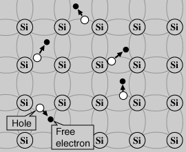
Metals tend to be good conductors of electricity because they usually have "free electrons" that can move easily between atoms, and electricity involves the flow of electrons. While silicon crystals look metallic, they are not, in fact, metals. All of the outer electrons in a silicon crystal are involved inperfect covalent bonds, so they can't move around. A pure silicon crystal is nearly an insulator -- very little electricity will