http://www.thebigger.com/physics/conductors-insulators-and-semi-conductors/what-are-extrinsic-semiconductors/
Extrinsic semiconductor
Those semiconductors in which someimpurity atoms are embedded are known as extrinsic semiconductors.
Extrinsic semi conductors are basically of two types:
1. P-type semi conductors
2. N-type semi conductors
1. P-type semi conductors
2. N-type semi conductors
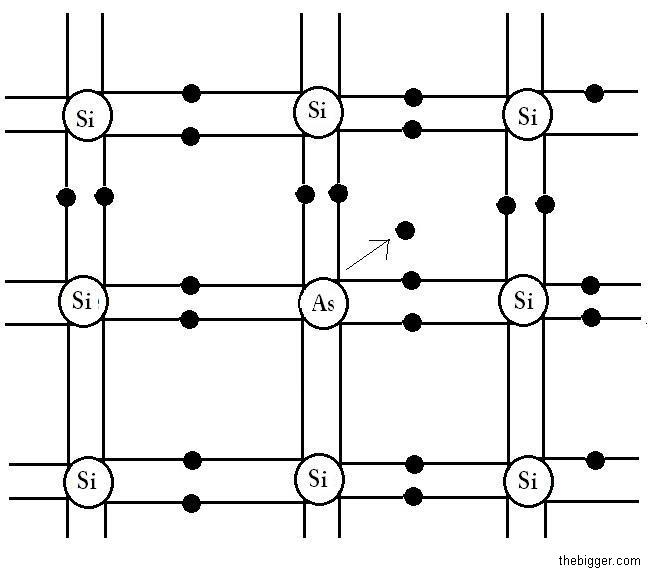
N-type Semi conductors: Let’s take an example of the silicon crystal to understand the concept of N-type semi conductor. We have studied the electronic configuration of the silicon atom. It has four electrons in its outermost shell. In N-type semi conductors, the silicon atoms are replaced with the pentavalent atoms like phosphorous, bismuth, antimony etc. So, as a result the four of the electrons of the pentavalent atoms will form the covalent bonds with the silicon atoms and the one electron will revolve around the nucleus of the impurity atoms with less binding energy. These electrons are almost free to move. In other words we can say that these electrons are donated by the impure atoms. So, these are also known as donor atoms. So, the conduction inside the conductor will take place with the help of the negatively charged electrons. Electrons are negatively charged. Due to this negative charge these semiconductors are known as N-type semiconductors.
Each donor atom has denoted an electron from its valence shell. So, as a result due to loss ofthe negative charge these atoms will become positively charged. The single valence electron revolves around the nucleus of the impure atom. Some experiments were performed. It was found that .01eV and .05eV energy is required to make the electron free from the nuclear forces.
When the semi conductors are placed at room temperature then the covalent bond breakage will take place. So, more free electrons will be generated. As a result, same no of holes generation will take place. But as compared to the free electrons the no of holes are comparatively less due to the presence of donor electrons.
We can say that major conduction of n-type semi conductors is due to electrons. So, electrons are known as majority carriers and the holes are known as the minority carriers.
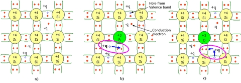
P-type semi conductors: In a p-type semi conductor doping is done with trivalent atoms .Trivalent atoms are those which have three valence electrons in their valence shell. Some examples of trivalent atoms are Aluminum, boron etc. So, the three valence electrons of the doped impure atoms will form the covalent bonds between silicon atoms. But silicon atoms have four electrons in its valence shell. So, one covalent bond will be improper. So, one more electron is needed for the proper covalent bonding. This need of one electron is fulfilled from any of the bond between two silicon atoms. So, the bond between the silicon and indium atom will be completed. After bond formation the indium will get ionized. As we know that ions are negatively charged. So, indium will also get negative charge. A hole was created when the electron come from silicon-silicon bond to complete the bond between indium and silicon. Now, an electron will move from any one of the covalent bond to fill the empty hole. This will result in a new holes formation. So, in p-type semi conductor the holes movement results in the formation of the current. Holes are positively charged. Hence these conductors are known as p-type semiconductors or acceptor type semi conductors.
When these conductors are placed at room temperature then the covalent bond breakage will take place. In this type of semi conductors the electrons are very less as compared to the holes. So, in p-type semi conductors holes are the majority carriers and electrons are the minority carriers.
Doped (extrinsic) semiconductors
An extrinsic semiconductor is a semiconductor doped by a specific impurity which is able to deeply modify its electrical properties, making it suitable for electronic applications (diodes, transistors, etc.) or optoelectronic applications (light emitters and detectors).
P-type semiconductors
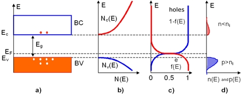
A P-type semiconductor is an intrinsic semiconductor (like Si) in which an impurity acting as an acceptor (like e.g. boron B in Si) has been intentionally added. These impurities are called acceptors since once they are inserted in the crystalline lattice, they lack one or several electrons to realize a full bonding with the rest of the crystal.
From figure 5, we see that a p-type semiconductor has a lower electron density n and a higher hole density p than the same intrinsic semiconductor. Electrons are said to be the minority carriers whereas holes are themajority carriers.
For extrinsic semiconductors, the dopant density is always far higher than the intrinsic carrier density : NA>>ni. In the case of a p-type material, the hole density is then close to the dopant density NA. Since the law of mass action is always true, we obtain the following expressions for the carrier densities
The Fermi level for a p-type semiconductor or chemical potential is then :
When the acceptor density is increased, the Fermi level moves closer to the edge of the valence band. If NA=Nv the Fermi level enters the valence band, the semiconductor is then said to be degenerate.
The important points regarding p-type semiconductors are summarized graphically in figure 6.
N-type semiconductors
A N-type semiconductor is an intrinsic semiconductor (e.g. silicon Si) in which a donor impurity (e.g. arsenic As in Si, or Si in GaAs) has been intentionally introduced. The impurities are called donor impurities since they have to give an extra electron to the conduction band in order to make all the bonds with neighboring atoms (As is pentavalent while Si is tetravalent).

From figure 7, we see that a n-type semiconductor has a higher electron density n and a lower hole density p than the same intrinsic semiconductor. Holes are said to be the minority carriers whereas electrons are themajority carriers.
Like in p-type semiconductors, we can write the following relationships, where ND is the donor density :
The Fermi level for a n-type semiconductor is then :
When the donor density is increased, the Fermi level moves closer to the edge of the conduction band. If ND=Nc the Fermi level enters the conduction band, the semiconductor is then said to be degenerate.
The important points regarding n-type semiconductors are summarized graphically in figure 8.
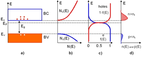
Figure 8 : N-type semiconductor
No comments:
Post a Comment