Friday, 11 January 2013
VLSI - An Introduction
http://www.kokanastha.com/career_guide/introduction_VLSI.html
VLSI - An Introduction
What is VLSI? VLSI stands for "Very Large Scale Integration". This is the field which involves packing more and more logic devices into smaller and smaller areas.Thanks to VLSI, circuits that would have taken boardfuls of space can now be put into a small space few millimeters across! This has opened up a big opportunity to do things that were not possible before. VLSI circuits are everywhere ... your computer, your car, your brand new state-of-the-art digital camera, the cell-phones, and what have you. All this involves a lot of expertise on many fronts within the same field, which we will look at in later sections. VLSI has been around for a long time, there is nothing new about it ... but as a side effect of advances in the world of computers, there has been a dramatic proliferation of tools that can be used to design VLSI circuits. Alongside, obeying Moore's law, the capability of an IC has increased exponentially over the years, in terms of computation power, utilisation of available area, yield. The combined effect of these two advances is that people can now put diverse functionality into the IC's, opening up new frontiers. Examples are embedded systems, where intelligent devices are put inside everyday objects, and ubiquitous computing where small computing devices proliferate to such an extent that even the shoes you wear may actually do something useful like monitoring your heartbeats! These two fields are kinda related, and getting into their description can easily lead to another article. | |||
DEALING WITH VLSI CIRCUITS
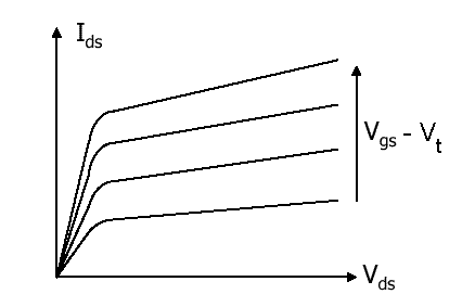
Digital VLSI circuits are predominantly CMOS based. The way normal blocks like latches and gates are implemented is different from what students have seen so far, but the behaviour remains the same. All the miniaturisation involves new things to consider. A lot of thought has to go into actual implementations as well as design. Let us look at some of the factors involved ... 1. Circuit Delays. Large complicated circuits running at very high frequencies have one big problem to tackle - the problem of delays in propagation of signals through gates and wires ... even for areas a few micrometers across! The operation speed is so large that as the delays add up, they can actually become comparable to the clock speeds. 2. Power. Another effect of high operation frequencies is increased consumption of power. This has two-fold effect - devices consume batteries faster, and heat dissipation increases. Coupled with the fact that surface areas have decreased, heat poses a major threat to the stability of the circuit itself. 3. Layout. Laying out the circuit components is task common to all branches of electronics. Whats so special in our case is that there are many possible ways to do this; there can be multiple layers of different materials on the same silicon, there can be different arrangements of the smaller parts for the same component and so on. The power dissipation and speed in a circuit present a trade-off; if we try to optimise on one, the other is affected. The choice between the two is determined by the way we chose the layout the circuit components. Layout can also affect the fabrication of VLSI chips, making it either easy or difficult to implement the components on the silicon. | |||
THE VLSI DESIGN PROCESS
A typical digital design flow is as follows: Specification Architecture RTL Coding RTL Verification Synthesis Backend Tape Out to Foundry to get end product….a wafer with repeated number of identical Ics. All modern digital designs start with a designer writing a hardware description of the IC (using HDL or Hardware Description Language) in Verilog/VHDL. A Verilog or VHDL program essentially describes the hardware (logic gates, Flip-Flops, counters etc) and the interconnect of the circuit blocks and the functionality. Various CAD tools are available to synthesize a circuit based on the HDL. The most widely used synthesis tools come from two CAD companies. Synposys and Cadence. Without going into details, we can say that the VHDL, can be called as the "C" of the VLSI industry. VHDL stands for "VHSIC Hardware Definition Language", where VHSIC stands for "Very High Speed Integrated Circuit". This languages is used to design the circuits at a high-level, in two ways. It can either be a behavioural description, which describes what the circuit is supposed to do, or a structural description, which describes what the circuit is made of. There are other languages for describing circuits, such as Verilog, which work in a similar fashion. Both forms of description are then used to generate a very low-level description that actually spells out how all this is to be fabricated on the silicon chips. This will result in the manufacture of the intended IC. A typical analog design flow is as follows: In case of analog design, the flow changes somewhat. Specifications Architecture Circuit Design SPICE Simulation Layout Parametric Extraction / Back Annotation Final Design Tape Out to foundry. While digital design is highly automated now, very small portion of analog design can be automated. There is a hardware description language called AHDL but is not widely used as it does not accurately give us the behavioral model of the circuit because of the complexity of the effects of parasitic on the analog behavior of the circuit. Many analog chips are what are termed as “flat” or non-hierarchical designs. This is true for small transistor count chips such as an operational amplifier, or a filter or a power management chip. For more complex analog chips such as data converters, the design is done at a transistor level, building up to a cell level, then a block level and then integrated at a chip level. Not many CAD tools are available for analog design even today and thus analog design remains a difficult art. SPICE remains the most useful simulation tool for analog as well as digital design. | |||
MOST OF TODAY’S VLSI DESIGNS ARE CLASSIFIED INTO THREE CATEGORIES:
1. Analog: Small transistor count precision circuits such as Amplifiers, Data converters, filters, Phase Locked Loops, Sensors etc. 2. ASICS or Application Specific Integrated Circuits: Progress in the fabrication of IC's has enabled us to create fast and powerful circuits in smaller and smaller devices. This also means that we can pack a lot more of functionality into the same area. The biggest application of this ability is found in the design of ASIC's. These are IC's that are created for specific purposes - each device is created to do a particular job, and do it well. The most common application area for this is DSP - signal filters, image compression, etc. To go to extremes, consider the fact that the digital wristwatch normally consists of a single IC doing all the time-keeping jobs as well as extra features like games, calendar, etc. 3. SoC or Systems on a chip: These are highly complex mixed signal circuits (digital and analog all on the same chip). A network processor chip or a wireless radio chip is an example of an SoC.
|
Integrated Circuit
http://www.techterms.com/definition/integratedcircuit
Integrated Circuit
An integrated circuit, or IC, is small chip that can function as an amplifier, oscillator, timer,microprocessor, or even computer memory. An IC is a small wafer, usually made of silicon, that can hold anywhere from hundreds to millions of transistors, resistors, and capacitors. These extremely small electronics can perform calculations and store data using either digital or analog technology.
Digital ICs use logic gates, which work only with values of ones and zeros. A low signal sent to to a component on a digital IC will result in a value of 0, while a high signal creates a value of 1. Digital ICs are the kind you will usually find in computers, networking equipment, and most consumer electronics.
Analog, or linear ICs work with continuous values. This means a component on a linear IC can take a value of any kind and output another value. The term "linear" is used since the output value is a linear function of the input. For example, a component on a linear IC may multiple an incoming value by a factor of 2.5 and output the result. Linear ICs are typically used in audio and radio frequency amplification.
Integrated circuit
"Silicon chip" redirects here. For the electronics magazine, see Silicon Chip.
"Microchip" redirects here. For other uses, see Microchip (disambiguation).


An integrated circuit or monolithic integrated circuit (also referred to as anIC, a chip, or a microchip) is a set of electronic circuits on one small plate ("chip") of semiconductor material, normally silicon. This can be made much smaller than a discrete circuit made from independent components.
Integrated circuits are used in virtually all electronic equipment today and have revolutionized the world of electronics. Computers, mobile phones, and other digital home appliances are now inextricable parts of the structure of modern societies, made possible by the low cost of producing integrated circuits.
ICs can be made very compact, having up to several billion transistors and otherelectronic components in an area the size of a fingernail. The width of each conducting line in a circuit (the line width) can be made smaller and smaller as the technology advances, in 2008 it dropped below 100 nanometers and in 2013 it is expected to be in the teens of nanometers.[1]
[edit]Introduction

ICs were made possible by experimental discoveries showing that semiconductor devices could perform the functions of vacuum tubes and by mid-20th-century technology advancements in semiconductor device fabrication. The integration of large numbers of tiny transistors into a small chip was an enormous improvement over the manual assembly of circuits using discrete electronic components. The integrated circuit's mass production capability, reliability, and building-block approach to circuit design ensured the rapid adoption of standardized Integrated Circuits in place of designs using discrete transistors.
There are two main advantages of ICs over discrete circuits: cost and performance. Cost is low because the chips, with all their components, are printed as a unit byphotolithography rather than being constructed one transistor at a time. Furthermore, much less material is used to construct a packaged IC die than to construct a discrete circuit. Performance is high because the components switch quickly and consume little power (compared to their discrete counterparts) as a result of the small size and close proximity of the components. As of 2012, typical chip areas range from a few square millimeters to around 450 mm2, with up to 9 million transistors per mm2.
[edit]Terminology
Integrated circuit originally referred to a miniaturized electronic circuit consisting of semiconductor devices, as well aspassive components bonded to a substrate or circuit board.[2] This configuration is now commonly referred to as a hybrid integrated circuit. Integrated circuit has since come to refer to the single-piece circuit construction originally known as amonolithic integrated circuit.[3]
[edit]Invention
Main article: Invention of the integrated circuit
Early developments of the integrated circuit go back to 1949, when the German engineer Werner Jacobi (Siemens AG) [4]filed a patent for an integrated-circuit-like semiconductor amplifying device[5] showing five transistors on a common substrate in a 2-stage amplifier arrangement. Jacobi disclosed small and cheap hearing aids as typical industrial applications of his patent. A commercial use of his patent has not been reported.
The idea of the integrated circuit was conceived by a radar scientist working for the Royal Radar Establishment of the BritishMinistry of Defence, Geoffrey W.A. Dummer (1909–2002). Dummer presented the idea to the public at the Symposium on Progress in Quality Electronic Components in Washington, D.C. on 7 May 1952.[6] He gave many symposia publicly to propagate his ideas, and unsuccessfully attempted to build such a circuit in 1956.
A precursor idea to the IC was to create small ceramic squares (wafers), each one containing a single miniaturized component. Components could then be integrated and wired into a bidimensional or tridimensional compact grid. This idea, which looked very promising in 1957, was proposed to the US Army by Jack Kilby, and led to the short-lived Micromodule Program (similar to 1951's Project Tinkertoy).[7] However, as the project was gaining momentum, Kilby came up with a new, revolutionary design: the IC.
Robert Noyce credited Kurt Lehovec of Sprague Electric for the principle of p-n junction isolation caused by the action of a biased p-n junction (the diode) as a key concept behind the IC.[8]

Newly employed by Texas Instruments, Kilby recorded his initial ideas concerning the integrated circuit in July 1958, successfully demonstrating the first working integrated example on 12 September 1958.[9] In his patent application of 6 February 1959, Kilby described his new device as “a body of semiconductor material ... wherein all the components of the electronic circuit are completely integrated.”[10] The first customer for the new invention was theUS Air Force.[11]
Kilby won the 2000 Nobel Prize in Physics for his part of the invention of the integrated circuit.[12] Kilby's work was named an IEEE Milestone in 2009.[13]
Noyce also came up with his own idea of an integrated circuit half a year later than Kilby. His chip solved many practical problems that Kilby's had not. Produced at Fairchild Semiconductor, it was made of silicon, whereas Kilby's chip was made of germanium.
Fairchild Semiconductor was also home of the first silicon gate IC technology with self-aligned gates, which stands as the basis of all modern CMOS computer chips. The technology was developed by Italian physicist Federico Faggin in 1968, who later joined Intel in order to develop the very first Central Processing Unit (CPU) on one chip (Intel 4004), for which he received the National Medal of Technology and Innovation in 2010.
[edit]Generations
In the early days of integrated circuits, only a few transistors could be placed on a chip, as the scale used was large because of the contemporary technology, and manufacturing yields were low by today's standards. As the degree of integration was small, the design process was relatively simple. Over time, millions, and today billions,[14] of transistors could be placed on one chip, and a good design required thorough planning. This gave rise to new design methods.
[edit]SSI, MSI and LSI
The first integrated circuits contained only a few transistors. Called "small-scale integration" (SSI), digital circuits containing transistors numbering in the tens provided a few logic gates for example, while early linear ICs such as thePlessey SL201 or the Philips TAA320 had as few as two transistors. The term Large Scale Integration was first used by IBMscientist Rolf Landauer when describing the theoretical concept[citation needed], from there came the terms for SSI, MSI, VLSI, and ULSI.
SSI circuits were crucial to early aerospace projects, and aerospace projects helped inspire development of the technology. Both the Minuteman missile and Apollo program needed lightweight digital computers for their inertial guidance systems; theApollo guidance computer led and motivated the integrated-circuit technology,[15] while the Minuteman missile forced it into mass-production. The Minuteman missile program and various other Navy programs accounted for the total $4 million integrated circuit market in 1962, and by 1968, U.S. Government space and defense spending still accounted for 37% of the $312 million total production. The demand by the U.S. Government supported the nascent integrated circuit market until costs fell enough to allow firms to penetrate the industrial and eventually the consumer markets. The average price per integrated circuit dropped from $50.00 in 1962 to $2.33 in 1968.[16] Integrated circuits began to appear in consumer products by the turn of the decade, a typical application being FM inter-carrier sound processing in television receivers.
The next step in the development of integrated circuits, taken in the late 1960s, introduced devices which contained hundreds of transistors on each chip, called "medium-scale integration" (MSI).
They were attractive economically because while they cost little more to produce than SSI devices, they allowed more complex systems to be produced using smaller circuit boards, less assembly work (because of fewer separate components), and a number of other advantages.
Further development, driven by the same economic factors, led to "large-scale integration" (LSI) in the mid 1970s, with tens of thousands of transistors per chip.
Integrated circuits such as 1K-bit RAMs, calculator chips, and the first microprocessors, that began to be manufactured in moderate quantities in the early 1970s, had under 4000 transistors. True LSI circuits, approaching 10,000 transistors, began to be produced around 1974, for computer main memories and second-generation microprocessors.
[edit]VLSI
Main article: Very-large-scale integration

The final step in the development process, starting in the 1980s and continuing through the present, was "very large-scale integration" (VLSI). The development started with hundreds of thousands of transistors in the early 1980s, and continues beyond several billion transistors as of 2009.
Multiple developments were required to achieve this increased density. Manufacturers moved to smaller design rules and cleaner fabrication facilities, so that they could make chips with more transistors and maintain adequate yield. The path of process improvements was summarized by the International Technology Roadmap for Semiconductors (ITRS). Design tools improved enough to make it practical to finish these designs in a reasonable time. The more energy efficient CMOS replaced NMOS and PMOS, avoiding a prohibitive increase in power consumption.
In 1986 the first one megabit RAM chips were introduced, which contained more than one million transistors. Microprocessor chips passed the million transistor mark in 1989 and the billion transistor mark in 2005.[17] The trend continues largely unabated, with chips introduced in 2007 containing tens of billions of memory transistors.[18]
[edit]ULSI, WSI, SOC and 3D-IC
Wafer-scale integration (WSI) is a system of building very-large integrated circuits that uses an entire silicon wafer to produce a single "super-chip". Through a combination of large size and reduced packaging, WSI could lead to dramatically reduced costs for some systems, notably massively parallel supercomputers. The name is taken from the term Very-Large-Scale Integration, the current state of the art when WSI was being developed.To reflect further growth of the complexity, the term ULSI that stands for "ultra-large-scale integration" was proposed for chips of complexity of more than 1 million transistors.
A system-on-a-chip (SoC or SOC) is an integrated circuit in which all the components needed for a computer or other system are included on a single chip. The design of such a device can be complex and costly, and building disparate components on a single piece of silicon may compromise the efficiency of some elements. However, these drawbacks are offset by lower manufacturing and assembly costs and by a greatly reduced power budget: because signals among the components are kept on-die, much less power is required (see Packaging).
A three-dimensional integrated circuit (3D-IC) has two or more layers of active electronic components that are integrated both vertically and horizontally into a single circuit. Communication between layers uses on-die signaling, so power consumption is much lower than in equivalent separate circuits. Judicious use of short vertical wires can substantially reduce overall wire length for faster operation.
[edit]Advances in integrated circuits

ICs have consistently migrated to smaller feature sizes over the years, allowing more circuitry to be packed on each chip. This increased capacity per unit area can be used to decrease cost and/or increase functionality—see Moore's law which, in its modern interpretation, states that the number of transistors in an integrated circuit doubles every two years. In general, as the feature size shrinks, almost everything improves—the cost per unit and the switching power consumption go down, and the speed goes up. However, ICs with nanometer-scale devices are not without their problems, principal among which is leakage current (see subthreshold leakage for a discussion of this), although these problems are not insurmountable and will likely be solved or at least ameliorated by the introduction of high-k dielectrics. Since these speed and power consumption gains are apparent to the end user, there is fierce competition among the manufacturers to use finer geometries. This process, and the expected progress over the next few years, is well described by the International Technology Roadmap for Semiconductors (ITRS).
In current research projects, integrated circuits are also developed for sensoric applications in medical implants or otherbioelectronic devices. Particular sealing strategies have to be taken in such biogenic environments to avoid corrosion orbiodegradation of the exposed semiconductor materials.[19] As one of the few materials well established in CMOStechnology, titanium nitride (TiN) turned out as exceptionally stable and well suited for electrode applications in medical implants.[20][21]
[edit]Classification

Digital integrated circuits can contain anything from one to millions of logic gates,flip-flops, multiplexers, and other circuits in a few square millimeters. The small size of these circuits allows high speed, low power dissipation, and reducedmanufacturing cost compared with board-level integration. These digital ICs, typically microprocessors, DSPs, and micro controllers, work using binary mathematics to process "one" and "zero" signals.
Analog ICs, such as sensors, power management circuits, and operational amplifiers, work by processing continuous signals. They perform functions like amplification, active filtering, demodulation, and mixing. Analog ICs ease the burden on circuit designers by having expertly designed analog circuits available instead of designing a difficult analog circuit from scratch.
ICs can also combine analog and digital circuits on a single chip to create functions such as A/D converters and D/A converters. Such mixed-signal circuits offer smaller size and lower cost, but must carefully account for signal interference.
Modern electronic component distributors often further sub-categorize the huge variety of integrated circuits now available:
- Digital ICs are further sub-categorized as logic ICs, memory chips, interface ICs ( level shifters, serializer/deserializer, etc.), Power Management ICs, and programmable devices.
- Analog ICs are further sub-categorized as linear ICs and RF ICs.
- mixed-signal integrated circuits are further sub-categorized as data acquisition ICs (including A/D converters, D/A converter, digital potentiometers) and clock/timing ICs.
[edit]Manufacturing
[edit]Fabrication
Main article: Semiconductor fabrication

.svg)
The semiconductors of the periodic table of the chemical elements were identified as the most likely materials for a solid-state vacuum tube. Starting with copper oxide, proceeding to germanium, then silicon, the materials were systematically studied in the 1940s and 1950s. Today, silicon monocrystals are the main substrate used for ICs although some III-V compounds of the periodic table such as gallium arsenideare used for specialized applications like LEDs, lasers, solar cells and the highest-speed integrated circuits. It took decades to perfect methods of creating crystalswithout defects in the crystalline structure of the semiconducting material.
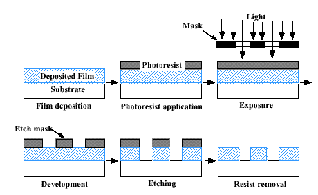
Semiconductor ICs are fabricated in a layer process which includes these key process steps:
- Imaging
- Deposition
- Etching
The main process steps are supplemented by doping and cleaning.
Mono-crystal silicon wafers (or for special applications, silicon on sapphire or gallium arsenide wafers) are used as the substrate. Photolithography is used to mark different areas of the substrate to be doped or to have polysilicon, insulators or metal (typically aluminium) tracks deposited on them.
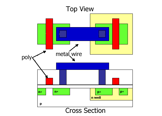
- Integrated circuits are composed of many overlapping layers, each defined by photolithography, and normally shown in different colors. Some layers mark where various dopants are diffused into the substrate (called diffusion layers), some define where additional ions are implanted (implant layers), some define the conductors (polysilicon or metal layers), and some define the connections between the conducting layers (via or contact layers). All components are constructed from a specific combination of these layers.
- In a self-aligned CMOS process, a transistor is formed wherever the gate layer (polysilicon or metal) crosses a diffusion layer.
- Capacitive structures, in form very much like the parallel conducting plates of a traditional electrical capacitor, are formed according to the area of the "plates", with insulating material between the plates. Capacitors of a wide range of sizes are common on ICs.
- Meandering stripes of varying lengths are sometimes used to form on-chipresistors, though most logic circuits do not need any resistors. The ratio of the length of the resistive structure to its width, combined with its sheet resistivity, determines the resistance.
- More rarely, inductive structures can be built as tiny on-chip coils, or simulated by gyrators.
Since a CMOS device only draws current on the transition between logic states, CMOS devices consume much less current than bipolar devices.
A random access memory is the most regular type of integrated circuit; the highest density devices are thus memories; but even a microprocessor will have memory on the chip. (See the regular array structure at the bottom of the first image.) Although the structures are intricate – with widths which have been shrinking for decades – the layers remain much thinner than the device widths. The layers of material are fabricated much like a photographic process, although light wavesin the visible spectrum cannot be used to "expose" a layer of material, as they would be too large for the features. Thusphotons of higher frequencies (typically ultraviolet) are used to create the patterns for each layer. Because each feature is so small, electron microscopes are essential tools for a process engineer who might be debugging a fabrication process.
Each device is tested before packaging using automated test equipment (ATE), in a process known as wafer testing, or wafer probing. The wafer is then cut into rectangular blocks, each of which is called a die. Each good die (plural dice, dies, or die) is then connected into a package using aluminium (or gold) bond wires which are welded and/or thermosonic bondedto pads, usually found around the edge of the die. After packaging, the devices go through final testing on the same or similar ATE used during wafer probing. Industrial CT scanning can also be used. Test cost can account for over 25% of the cost of fabrication on lower cost products, but can be negligible on low yielding, larger, and/or higher cost devices.
As of 2005, a fabrication facility (commonly known as a semiconductor fab) costs over US$1 billion to construct,[22]because much of the operation is automated. Today, the most advanced processes employ the following techniques:
- The wafers are up to 300 mm in diameter (wider than a common dinner plate).
- Use of 32 nanometer or smaller chip manufacturing process. Intel, IBM, NEC, and AMD are using ~32 nanometers for their CPU chips. IBM and AMD introduced immersion lithography for their 45 nm processes[23]
- Copper interconnects where copper wiring replaces aluminium for interconnects.
- Low-K dielectric insulators.
- Silicon on insulator (SOI)
- Strained silicon in a process used by IBM known as strained silicon directly on insulator (SSDOI)
- Multigate devices such as tri-gate transistors being manufactured by Intel from 2011 in their 22 nm process.
[edit]Packaging
Main article: Integrated circuit packaging

The earliest integrated circuits were packaged in ceramic flat packs, which continued to be used by the military for their reliability and small size for many years. Commercial circuit packaging quickly moved to the dual in-line package(DIP), first in ceramic and later in plastic. In the 1980s pin counts of VLSI circuits exceeded the practical limit for DIP packaging, leading to pin grid array (PGA) and leadless chip carrier (LCC) packages. Surface mount packaging appeared in the early 1980s and became popular in the late 1980s, using finer lead pitch with leads formed as either gull-wing or J-lead, as exemplified by small-outline integrated circuit – a carrier which occupies an area about 30–50% less than an equivalent DIP, with a typical thickness that is 70% less. This package has "gull wing" leads protruding from the two long sides and a lead spacing of 0.050 inches.
In the late 1990s, plastic quad flat pack (PQFP) and thin small-outline package(TSOP) packages became the most common for high pin count devices, though PGA packages are still often used for high-end microprocessors. Intel and AMD are currently transitioning from PGA packages on high-end microprocessors to land grid array (LGA) packages.
Ball grid array (BGA) packages have existed since the 1970s. Flip-chip Ball Grid Array packages, which allow for much higher pin count than other package types, were developed in the 1990s. In an FCBGA package the die is mounted upside-down (flipped) and connects to the package balls via a package substrate that is similar to a printed-circuit board rather than by wires. FCBGA packages allow an array of input-output signals (called Area-I/O) to be distributed over the entire die rather than being confined to the die periphery.
Traces out of the die, through the package, and into the printed circuit board have very different electrical properties, compared to on-chip signals. They require special design techniques and need much more electric power than signals confined to the chip itself.
When multiple dies are put in one package, it is called SiP, for System In Package. When multiple dies are combined on a small substrate, often ceramic, it's called an MCM, or Multi-Chip Module. The boundary between a big MCM and a small printed circuit board is sometimes fuzzy.
[edit]Chip labeling and manufacture date
Most integrated circuits large enough to include identifying information include four common sections: the manufacturer's name or logo, the part number, a part production batch number and/or serial number, and a four-digit code that identifies when the chip was manufactured. Extremely small surface mount technology parts often bear only a number used in a manufacturer's lookup table to find the chip characteristics.
The manufacturing date is commonly represented as a two-digit year followed by a two-digit week code, such that a part bearing the code 8341 was manufactured in week 41 of 1983, or approximately in October 1983.
[edit]Legal protection of semiconductor chip layouts
Main article: Integrated circuit layout design protection
Like most of the other forms of intellectual property, IC layout designs are creations of the human mind. They are usually the result of an enormous investment, both in terms of the time of highly qualified experts, and financially. There is a continuing need for the creation of new layout-designs which reduce the dimensions of existing integrated circuits and simultaneously increase their functions. The smaller an integrated circuit, the less the material needed for its manufacture, and the smaller the space needed to accommodate it. Integrated circuits are utilized in a large range of products, including articles of everyday use, such as watches, television sets, appliances, automobiles, etc., as well as sophisticated data processing equipment.
The possibility of copying by photographing each layer of an integrated circuit and preparing photomasks for its production on the basis of the photographs obtained is the main reason for the introduction of legislation for the protection of layout-designs.
A diplomatic conference was held at Washington, D.C., in 1989, which adopted a Treaty on Intellectual Property in Respect of Integrated Circuits (IPIC Treaty).
The Treaty on Intellectual Property in respect of Integrated Circuits, also called Washington Treaty or IPIC Treaty (signed at Washington on 26 May 1989) is currently not in force, but was partially integrated into the TRIPS agreement.
National laws protecting IC layout designs have been adopted in a number of countries.
[edit]Other developments
In the 1980s, programmable logic devices were developed. These devices contain circuits whose logical function and connectivity can be programmed by the user, rather than being fixed by the integrated circuit manufacturer. This allows a single chip to be programmed to implement different LSI-type functions such as logic gates, adders and registers. Current devices called field-programmable gate arrays can now implement tens of thousands of LSI circuits in parallel and operate up to 1.5 GHz (Achronix holding the speed record).
The techniques perfected by the integrated circuits industry over the last three decades have been used to create very small mechanical devices driven by electricity using a technology known as microelectromechanical systems. These devices are used in a variety of commercial and military applications. Example commercial applications include DLP projectors, inkjet printers, and accelerometers used to deploy automobile airbags.
In the past, radios could not be fabricated in the same low-cost processes as microprocessors. But since 1998, a large number of radio chips have been developed using CMOS processes. Examples include Intel's DECT cordless phone, orAtheros's 802.11 card.
Future developments seem to follow the multi-core multi-microprocessor paradigm, already used by the Intel and AMD dual-core processors. Rapport Inc. and IBM started shipping the KC256 in 2006, a 256-core microprocessor. Intel, as recently as February-August 2011, unveiled a prototype, "not for commercial sale" chip that bears 80 cores. Each core is capable of handling its own task independently of the others. This is in response to the heat-versus-speed limit that is about to be reached using existing transistor technology (see: thermal design power ). This design provides a new challenge to chip programming. Parallel programming languages such as the open-source X10 programming language are designed to assist with this task.[25]
Since the early 2000s, the integration of optical functionality into silicon chips has been actively pursued in both academic research and in industry resulting in the successful commercialization of silicon based integrated optical transceivers combining optical devices (modulators, detectors, routing) with CMOS based electronics.[26]
[edit]Silicon labelling and graffiti
To allow identification during production most silicon chips will have a serial number in one corner. It is also common to add the manufacturer's logo. Ever since ICs were created, some chip designers have used the silicon surface area for surreptitious, non-functional images or words. These are sometimes referred to as Chip Art, Silicon Art, Silicon Graffiti orSilicon Doodling.
[edit]ICs and IC families
- The 555 timer IC
- The 741 operational amplifier
- 7400 series TTL logic building blocks
- 4000 series, the CMOS counterpart to the 7400 series (see also: 74HC00 series)
- Intel 4004, the world's first microprocessor, which led to the famous 8080 CPU and then the IBM PC's 8088, 80286, 486etc.
- The MOS Technology 6502 and Zilog Z80 microprocessors, used in many home computers of the early 1980s
- The Motorola 6800 series of computer-related chips, leading to the 68000 and 88000 series (used in some Apple computers and in the 1980s Commodore Amiga series).
Subscribe to:
Comments (Atom)