Intrinsic semiconductor
n
(Electronics) an almost pure semiconductor to which no impurities have been added and in which the electron and hole densities are equal at thermal equilibrium Also called i-type semiconductor
http://hyperphysics.phy-astr.gsu.edu/hbase/solids/intrin.html
Intrinsic Semiconductor
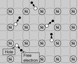
A silicon crystal is different from an insulator because at any temperature above absolute zero temperature, there is a finite probability that an electron in the lattice will be knocked loose from its position, leaving behind an electron deficiency called a "hole".
If a voltage is applied, then both the electron and the hole can contribute to a small current flow.
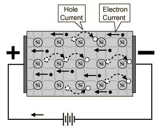
 The conductivity of a semiconductor can be modeled in terms of the band theory of solids. The band model of a semiconductor suggests that at ordinary temperatures there is a finite possibility that electrons can reach the conduction bandand contribute to electrical conduction. The conductivity of a semiconductor can be modeled in terms of the band theory of solids. The band model of a semiconductor suggests that at ordinary temperatures there is a finite possibility that electrons can reach the conduction bandand contribute to electrical conduction.The term intrinsic here distinguishes between the properties of pure "intrinsic" silicon and the dramatically different properties of doped n-type or p-typesemiconductors. Electrons and holes Semiconductor Current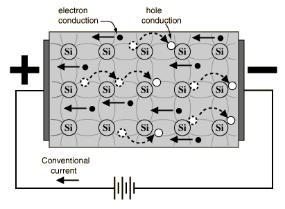 Semiconductor CurrentThe current which will flow in an intrinsic semiconductor consists of bothelectron and hole current. That is, the electrons which have been freed from their lattice positions into the conduction band can move through the material.
The current flow in an intrinsic semiconductor is influenced by the density of energy states which in turn influences the electron density in the conduction band. This current is highly temperature dependent.
Electrons and HolesIn an intrinsic semiconductor like silicon at temperatures above absolute zero, there will be some electrons which are excited across the band gap into the conduction band and which can produce current. When the electron in pure silicon crosses the gap, it leaves behind an electron vacancy or "hole" in the regular silicon lattice. Under the influence of an external voltage, both the electron and the hole can move across the material. In an n-typesemiconductor, the dopant contributes extra electrons, dramatically increasing the conductivity. In a p-type semiconductor, the dopant produces extra vacancies or holes, which likewise increase the conductivity. It is however the behavior of the p-n junction which is the key to the enormous variety of solid-state electronic devices.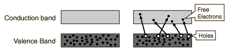
|
http://www.optique-ingenieur.org/en/courses/OPI_ang_M05_C02/co/Contenu_03.html
Intrinsic semiconductors
An intrinsic semiconductor is an undoped semiconductor. This means that holes in the valence band are vacancies created by electrons that have been thermally excited to the conduction band, as opposed to doped semiconductors where holes or electrons are supplied by a “foreign” atom acting as an impurity.
In order to better understand the behavior of semiconductors, we need to investigate more deeply what are the electron and hole densities in the conduction and valence bands, respectively. We first need to introduce the notion of energydensity of states N(E). This parameter gives the number of states (per unit volume and per unit energy) between E and E+dE: Nc(E) (respectively, Nv(E)) physically represents the “room” available for electrons (resp. holes) in the conduction band (resp. valence band). For energies that are close to the extrema of these two bands, the density of states has a quadratic dependence with E:
Where  is the normalized Planck constant (h=6.626.10-34Js) and mc(resp. mv) is the average effective mass of the conduction band (resp. of the valence band). For a direct gap semiconductor, mc (resp. mv) is the effective mass of an electron me (resp. a hole mh) in the crystal.
is the normalized Planck constant (h=6.626.10-34Js) and mc(resp. mv) is the average effective mass of the conduction band (resp. of the valence band). For a direct gap semiconductor, mc (resp. mv) is the effective mass of an electron me (resp. a hole mh) in the crystal.
The above-mentioned concept of effective mass allows considering electrons (and holes) inside the crystal as almost free particles, like free quasi-particles. The semiconductor then becomes an electron (and hole) gas, but in which electrons and holes have an effective mass which may be very different of the mass of the particle moving in free space. For example, for GaAs mc/m0=0,066 avec m0=0,911.10-30kg is the free electron mass.
In order to know what is the number of electrons and holes present in each band, the density of states is not the only information that we need. We also have to know the probability for an electron to occupy a level with a given energy E. This probability is given by the Fermi-Dirac distribution function :
Where k=1,38.10-23 JK-1 is the Boltzmann constant, T the temperature and EF the Fermi energy, which is the chemical potential for semiconductors.
The probability for a hole to occupy a level of energy E is simply given by 1-f(E) since a hole is by definition the absence of an electron.
The electron density n [cm-3] in the conduction band is obtained by integrating, over the range of energies accessible by electrons in the band, the number of states that may be occupied by electrons of energy E, weighted by the probability to “find” an electron having this given energy :
Similarly, the hole density p [cm-3] in the valence band writes :
For a semiconductor whose Fermi level EF is located more than 3 kT away from the extrema, the Fermi distribution function can be written under the form of a simple exponential, so that the expressions for the charge carriers densities become :
Where Nc et Nv are called the effective densities of states. They represent the density of “useful” states, at a given temperature T, in their respective energy band.
Let's note that the product of the two densities turns out to be independent on the position of the Fermi level. This is still true even for extrinsic semiconductors (see below). It is known as the law of mass action since it resembles the law of mass action encountered in chemistry (for instance the auto-ionization equilibrium of water is governed by [H+][OH-]=Ke).
Where ni is the density of intrinsic carriers (for Si at 300K, ni 1010cm-3).
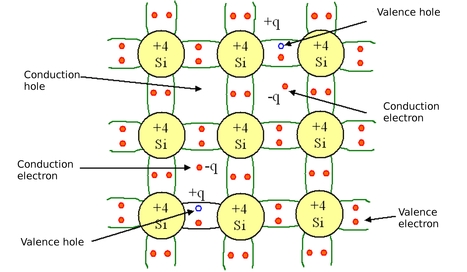
Figure 3 shows that for an intrinsic semiconductor (without impurities), each electron in the conduction band is associated with a hole in the valence band. We conclude that the electron and hole densities are equal :
By substituting the carrier densities by their respective expressions, this relationship allows defining the Fermi level for an intrinsic semiconductor EFi. Since at room temperature kT is significantly lower than the energy gap, this level is located near the middle of the forbidden band :
In figure 4 are graphically summarized the important points raised above for intrinsic semiconductors.
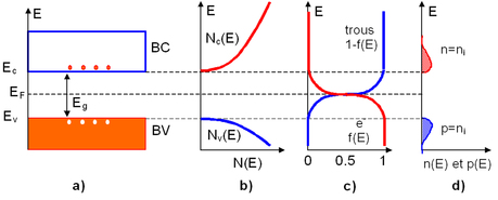
Figure 4 : Intrinsic semiconductor
No comments:
Post a Comment