http://en.wikipedia.org/wiki/Field-effect_transistor
Field-effect transistor
From Wikipedia, the free encyclopedia
"FET" redirects here. For other uses, see FET (disambiguation).
| This article needs additional citations for verification. (December 2010) |

The field-effect transistor (FET) is a transistor that uses an electric field to control the shape and hence the conductivity of a channel of one type of charge carrier in asemiconductor material. FETs are unipolar transistors as they involve single-carrier-type operation. The concept of the FET predates the Bipolar junction transistor (BJT), though it was not physically implemented until after BJTs due to the limitations of semiconductor materials and the relative ease of manufacturing BJTs compared to FETs at the time.
Contents[hide] |
[edit]History
Main article: History of the transistor
The field-effect transistor was first patented by Julius Edgar Lilienfeld in 1925 and by Oskar Heil in 1934, but practical semi-conducting devices (the JFET) were only developed much later after the transistor effect was observed and explained by the team of William Shockley at Bell Labs in 1947. The MOSFET, which largely superseded the JFET and had a more profound effect on electronic development, was first proposed by Dawon Kahng in 1960.[1]
[edit]Basic information
FETs are majority-charge-carrier devices. The device consists of an active channel through which majority charge carriers, electrons or holes, flow from the source to the drain. Source and drain terminal conductors are connected to the semiconductor through ohmic contacts. The conductivity of the channel is a function of potential applied across the gate and source terminals.
The FET's three terminals are:[2]
- Source (S), through which the majority carriers enter the channel. Conventional current entering the channel at S is designated by IS.
- Drain (D), through which the majority carriers leave the channel. Conventional current entering the channel at D is designated by ID. Drain to Source voltage is VDS.
- Gate (G), the terminal that modulates the channel conductivity. By applying voltage to G, one can control ID.
[edit]More about terminals

All FETs have source, drain, and gate terminals that correspond roughly to the emitter, collector, and base of BJTs. Most FETs have a fourth terminal called the body, base, bulk, or substrate.This fourth terminal serves to bias the transistor into operation; it is rare to make non-trivial use of the body terminal in circuit designs, but its presence is important when setting up the physical layout of an integrated circuit. The size of the gate, length L in the diagram, is the distance between source and drain. The width is the extension of the transistor, in the diagram perpendicular to the cross section. Typically the width is much larger than the length of the gate. A gate length of 1 µm limits the upper frequency to about 5 GHz, 0.2 µm to about 30 GHz.
The names of the terminals refer to their functions. The gate terminal may be thought of as controlling the opening and closing of a physical gate. This gate permits electrons to flow through or blocks their passage by creating or eliminating a channel between the source and drain. Electrons flow from the source terminal towards the drain terminal if influenced by an applied voltage. The body simply refers to the bulk of the semiconductor in which the gate, source and drain lie. Usually the body terminal is connected to the highest or lowest voltage within the circuit, depending on type. The body terminal and the source terminal are sometimes connected together since the source is also sometimes connected to the highest or lowest voltage within the circuit, however there are several uses of FETs which do not have such a configuration, such as transmission gates and cascode circuits.
[edit]FET operation
See also: Field effect (semiconductor)

The FET controls the flow of electrons (or electron holes) from the source to drain by affecting the size and shape of a "conductive channel" created and influenced by voltage (or lack of voltage) applied across the gate and source terminals. (For ease of discussion, this assumes body and source are connected.) This conductive channel is the "stream" through which electrons flow from source to drain.
In an n-channel depletion-mode device, a negative gate-to-source voltage causes adepletion region to expand in width and encroach on the channel from the sides, narrowing the channel. If the depletion region expands to completely close the channel, the resistance of the channel from source to drain becomes large, and the FET is effectively turned off like a switch. Likewise a positive gate-to-source voltage increases the channel size and allows electrons to flow easily.
Conversely, in an n-channel enhancement-mode device, a positive gate-to-source voltage is necessary to create a conductive channel, since one does not exist naturally within the transistor. The positive voltage attracts free-floating electrons within the body towards the gate, forming a conductive channel. But first, enough electrons must be attracted near the gate to counter the dopant ions added to the body of the FET; this forms a region free of mobile carriers called a depletion region, and the phenomenon is referred to as the threshold voltage of the FET. Further gate-to-source voltage increase will attract even more electrons towards the gate which are able to create a conductive channel from source to drain; this process is called inversion.
In a p-channel depletion-mode device, a positive voltage from gate to body creates a depletion layer by forcing the positively charged holes away from the gate-insulator/semiconductor interface, leaving exposed a carrier-free region of immobile, negatively charged acceptor ions.
For either enhancement- or depletion-mode devices, at drain-to-source voltages much less than gate-to-source voltages, changing the gate voltage will alter the channel resistance, and drain current will be proportional to drain voltage (referenced to source voltage). In this mode the FET operates like a variable resistor and the FET is said to be operating in a linear mode or ohmic mode.[3][4]
If drain-to-source voltage is increased, this creates a significant asymmetrical change in the shape of the channel due to a gradient of voltage potential from source to drain. The shape of the inversion region becomes "pinched-off" near the drain end of the channel. If drain-to-source voltage is increased further, the pinch-off point of the channel begins to move away from the drain towards the source. The FET is said to be in saturation mode;[5] some authors refer to it as active mode, for a better analogy with bipolar transistor operating regions.[6][7] The saturation mode, or the region between ohmic and saturation, is used when amplification is needed. The in-between region is sometimes considered to be part of the ohmic or linear region, even where drain current is not approximately linear with drain voltage.
Even though the conductive channel formed by gate-to-source voltage no longer connects source to drain during saturation mode,carriers are not blocked from flowing. Considering again an n-channel device, a depletion region exists in the p-type body, surrounding the conductive channel and drain and source regions. The electrons which comprise the channel are free to move out of the channel through the depletion region if attracted to the drain by drain-to-source voltage. The depletion region is free of carriers and has a resistance similar to silicon. Any increase of the drain-to-source voltage will increase the distance from drain to the pinch-off point, increasing resistance due to the depletion region proportionally to the applied drain-to-source voltage. This proportional change causes the drain-to-source current to remain relatively fixed independent of changes to the drain-to-source voltage and quite unlike the linear mode operation. Thus in saturation mode, the FET behaves as a constant-current source rather than as a resistor and can be used most effectively as a voltage amplifier. In this case, the gate-to-source voltage determines the level of constant current through the channel.
[edit]Composition
The FET can be constructed from a number of semiconductors, silicon being by far the most common. Most FETs are made with conventional bulk semiconductor processing techniques, using a single crystal semiconductor wafer as the active region, or channel.
Among the more unusual body materials are amorphous silicon, polycrystalline silicon or other amorphous semiconductors in thin-film transistors or organic field effect transistors that are based on organic semiconductors; often, OFET gate insulators and electrodes are made of organic materials, as well. Such FETs are manufactured using variety of materials such as silicon carbide(SiC), gallium arsenide(GaAs), gallium nitride(GaN), and indium gallium arsenide(InGaAs). In June 2011, IBM announced that it had successfully usedgraphene-based FETs in an integrated circuit.[8][9] These transistors are capable of about 2.23 GHz cutoff frequency, much higher than standard silicon FETs.[10]
[edit]Types of field-effect transistors

The channel of a FET is doped to produce either an N-type semiconductor or aP-type semiconductor. The drain and source may be doped of opposite type to the channel, in the case of depletion mode FETs, or doped of similar type to the channel as in enhancement mode FETs. Field-effect transistors are also distinguished by the method of insulation between channel and gate. Types of FETs are:
- CNTFET (Carbon nanotube field-effect transistor)
- The DEPFET is a FET formed in a fully depleted substrate and acts as a sensor, amplifier and memory node at the same time. It can be used as an image (photon) sensor.
- The DGMOSFET is a MOSFET with dual gates.
- The DNAFET is a specialized FET that acts as a biosensor, by using a gate made of single-strand DNA molecules to detect matching DNA strands.
- The FREDFET (Fast Reverse or Fast Recovery Epitaxial Diode FET) is a specialized FET designed to provide a very fast recovery (turn-off) of the body diode.
- The HEMT (high electron mobility transistor), also called a HFET (heterostructure FET), can be made using bandgap engineering in a ternary semiconductor such as AlGaAs. The fully depleted wide-band-gap material forms the isolation between gate and body.
- The HIGFET (heterostructure insulated gate field effect transisitor), is used mainly in research now. [1]
- The IGBT (insulated-gate bipolar transistor) is a device for power control. It has a structure akin to a MOSFET coupled with a bipolar-like main conduction channel. These are commonly used for the 200-3000 V drain-to-source voltage range of operation. Power MOSFETs are still the device of choice for drain-to-source voltages of 1 to 200 V.
- The ISFET (ion-sensitive field-effect transistor) used to measure ion concentrations in a solution; when the ion concentration (such as H+, see pH electrode) changes, the current through the transistor will change accordingly.
- The JFET (junction field-effect transistor) uses a reverse biased p-n junction to separate the gate from the body.
- The MESFET (Metal–Semiconductor Field-Effect Transistor) substitutes the p-n junction of the JFET with a Schottky barrier; used in GaAs and other III-V semiconductor materials.
- The MODFET (Modulation-Doped Field Effect Transistor) uses a quantum well structure formed by graded doping of the active region.
- The MOSFET (Metal–Oxide–Semiconductor Field-Effect Transistor) utilizes an insulator (typically SiO2) between the gate and the body.
- The NOMFET is a Nanoparticle Organic Memory Field-Effect Transistor.[2]
- The OFET is an Organic Field-Effect Transistor using an organic semiconductor in its channel.
- The GNRFET is a Field-Effect Transistor that uses a graphene nanoribbon for its channel.
- The VeSFET (Vertical-Slit Field-Effect Transistor) is a square-shaped junction-less FET with a narrow slit connecting the source and drain at opposite corners. Two gates occupy the other corners, and control the current through the slit. [3] [4]
- The TFET (Tunnel Field-Effect Transistor) is based on band to band tunneling [11]
[edit]Advantages of FET
The main advantage of the FET is its high input resistance, on the order of 100M ohms or more. Thus, it is a voltage-controlled device, and shows a high degree of isolation between input and output. It is a unipolar device, depending only upon majority current flow. It is less noisy and is thus found in FM tuners for quiet reception. It is relatively immune to radiation. It exhibits no offset voltage at zero drain current and hence makes an excellent signal chopper. It typically has better thermal stability than a BJT.[2]
[edit]Advantages of FET over "BJT"
- Very high input impedance ( In the order of Mego )
- FET is unipolar
- High miniaturisation is possible
- Very high switching speed
- FET is less noisy
- Low temperature sensitivity
- FET is voltage controlled device
- The characteristics will not change with time
[edit]Disadvantages of FET
It has relatively low gain-bandwidth product compared to a BJT. The MOSFET has a drawback of being very susceptible to overload voltages, thus requiring special handling during installation.[12]
[edit]Uses
IGBTs see application in switching internal combustion engine ignition coils, where fast switching and voltage blocking capabilities are important.
The most commonly used FET is the MOSFET. The CMOS (complementary metal oxide semiconductor) process technology is the basis for modern digital integrated circuits. This process technology uses an arrangement where the (usually "enhancement-mode") p-channel MOSFET and n-channel MOSFET are connected in series such that when one is on, the other is off.
The fragile insulating layer of the MOSFET between the gate and channel makes it vulnerable to electrostatic damage during handling. This is not usually a problem after the device has been installed in a properly designed circuit.
In FETs electrons can flow in either direction through the channel when operated in the linear mode, and the naming convention of drain terminal and source terminal is somewhat arbitrary, as the devices are typically (but not always) built symmetrically from source to drain. This makes FETs suitable for switching analog signals between paths (multiplexing). With this concept, one can construct a solid-state mixing board, for example.
A common use of the FET is as an amplifier. For example, due to its large input resistance and low output resistance, it is effective as a buffer in common-drain (source follower) configuration.
http://www.slideshare.net/guest3b5d8a/fieldeffect-transistors
Field-Effect Transistors
- 1. Field-Effect Transistors
- 2. Field-effect transistors General overview Types of field-effect transistors Uses
- 3. 1. General overview Field-effect transistors (FETs) follow an other principle than bipolar junction transistors They rely on an electric field to control the shape and hence the conductivity of a „channel“ in a semiconductor material FETs controlled by voltage ( BJTs controlled by current)
- 4. 1. General overview The concept of the field effect transistor predates the bipolar junction transistor (BJT) Was not physically implemented until after BJTs, due to limitations of semiconductor materials and relative ease of manufacturing BJTs compared to FETs at that time.
- 5. 1. General overview Basic principle of FETs The terminals of a FET refer to their function: Gate (G), Source (S), Drain (D) control terminal current channel of charge carriers for charge carriers control voltage
- 6. 1. General overview FETs are voltage-controlled by the voltage between gate and source terminal Voltage effects the electric field of the transistor which enlarges or diminishes the channel Effects the current stream through the FET
- 7. 2. Types of field-effect transistors Junction Field-Effect Transistors JFETs Simplest type of FET Long channel semiconductor Either p- or n-doped ( p-type, n-type) A contact at each end source and drain terminals Gate terminal surrounds the channel and is doped opposite to the doping of the channel
- 8. 2. Types of field-effect transistors Junction Field-Effect Transistors JFETs N-channel types and P-channel types
- 9. 2. Types of field-effect transistors Metal-Oxide-Semiconductor FETs MOS-FETs Most common field-effect transistor traditional metal–oxide–semiconductor (MOS) structure is obtained by depositing a layer of silicon dioxide and a layer of metal on top of a semiconductor die. As the silicon dioxide is a dielectric material its structure is equivalent to a planar capacitor, with one of the electrodes replaced by a semiconductor (substrate)
- 10. 2. Types of field-effect transistors Metal-Oxide-Semiconductor FETs MOS-FETs Metal electrode is used as the gate, the other forms the so called body/bulk/substrate terminal of a MOS-FET Opposite doted semiconductors placed within the substrate form the drain and source terminals Modulating the MOS-Capacitance forms a channel between source and drain terminals This controls the current flow through the MOS-FET
- 11. 2. Types of field-effect transistors Metal-Oxide-Semiconductor FETs MOS-FETs
- 12. 2. Types of field-effect transistors Metal-Oxide-Semiconductor FETs MOS-FETs depletion-mode enhancement-mode P-Channel N-Channel
- 13. 3. Uses As well as BJTs, FETs can be used as switching and/or amplifying elements JFETs are also often used as variable, controlable resistors FETs, especially JFETs consumpt almost no current high input impedance Makes JFETs very suitable for pre-amplifiers FETs behave like electron tubes from the old days Integrated circuits (CMOS, other modern elements) use MOS-FETs as the switching element Power-MOS-FETs are used in HiFi power amplifiers and produce a sound comparable to tube amplifiers Many, many more uses…

The control terminal is called the gate. Remember that the base terminal of a bipolar transistor passes a small amount of current. The gate on the FET passes virtually no current when driven with D.C. When driving the gate with high frequency pulsed D.C. or A.C. there may be a small amount of current flow. The transistor's "turn on" (a.k.a. threshold) voltage varies from one FET to another but is approximately 3.3 volts with respect to the source.
When FETs are used in the audio output section of an amplifier, the Vgs (voltage from gate to source) is rarely higher than 3.5 volts. When FETs are used in switching power supplies, the Vgs is usually much higher (10 to 15 volts). When the gate voltage is above approximately 5 volts, it becomes more efficient (which means less voltage drop across the FET and therefore less power dissipation).
MOSFETs are commonly used because they are easier to drive in high current applications (such as the switching power supplies found in car audio amplifiers). If a bipolar transistor is used, a fraction of the collector/emitter current must flow through the base junction. In high current situations where there is significant collector/emitter current, the base current may be significant. FETs can be driven by very little current (compared to the bipolar transistors). The only current that flows from the drive circuit is the current that flows due to the capacitance. As you already know, when DC is applied to a capacitor, there is an initial surge then the current flow stops. When the gate of an FET is driven with a high frequency signal, the drive circuit essentially sees only a small value capacitor. For low to intermediate frequencies, the drive circuit has to deliver little current. At very high frequencies or when many FETs are being driven, the drive circuit must be able to deliver more current.
Note:
The gate of a MOSFET has some capacitance which means that it will hold a charge (retain voltage). If the gate voltage is not discharged, the FET will continue to conduct current. This doesn't mean you can charge it and expect the FET to continue to conduct indefinitely but it will continue to conduct until the voltage on the gate is below the threshold voltage. You can make sure it turns off if you connect a pulldown resistor between the gate and source.
High Current Terminals:
The 'controlled' terminals are called the source and the drain. These are the terminals responsible for conducting the current through the transistor.
Transistor Packages:
The MOSFETs use the same 'packages' as bipolar transistors. The most common in car stereo amplifiers is currently the TO-220 package (shown above).
Transistor In Circuit:
This diagram shows the voltages across the resistor and the FET with 3 different gate voltages. You should see that there is no voltage across the resistor when the gate voltage is around 2.5 volts. This means that there is no current flowing because the transistor is not turned on. When the transistor is partially turned on, there is a voltage drop (voltage) across both components. When the transistor is fully turned on (gate voltage approx. 4.5 volts), the full supply voltage is across the resistor and there is virtually no voltage drop across the transistor. This means that both terminals (source and drain) of the transistor have essentially the same voltage. When the transistor is fully turned on, the lower lead of the resistor is effectively connected to ground.
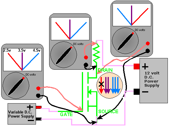
| Voltage applied to gate | Voltage across resistor | Voltage across transistor |
| 2.5 volts | no voltage | approximately 12 volts |
| 3.5 volts | less than 12 volts | less than 12 volts |
| 4.5 volts | approximately 12 volts | virtually no voltage |
In the following demo, you can see that there is an FET connected to a lamp. When the voltage is below about 3 volts, the lamp is completely off. There is no current flowing through the lamp or the FET. When you push the button, you can see that the capacitor starts to charge (indicated by the rising yellow line and by the point where the capacitor's charging curve intersects with the white line sweeping from left to right. When the FET starts to turn on, the voltage on the drain starts to fall (indicated by the falling green line and the point where the green curve intersects with the white line). As the gate voltage approaches the threshold voltage (~3.5v), the voltage across the lamp starts to increase. The more it increases, the brighter the lamp becomes. After the voltage on the gate reaches about 4 volts, you can see that the bulb is fully on (it has the full 12 volts across its terminals). There is virtually no voltage across the FET. You should notice that the FET is fully off below 3 volts and fully on after 4 volts. Any gate voltage below 3 volts has virtually no effect on the FET. Above 4 volts, there is little effect.
As you already know, the FET is controlled by its gate voltage. For this type of MOSFET the maximum safe gate voltage is ±20 volts. If more than 20 volts is applied to the gate (referenced to the source) it will destroy the transistor. The transistor will be damaged because the voltage will arc through the insulator that separates the gate from the drain/source part of the FET.
Current:
As with bipolar transistors, each FET is designed to safely pass a specified amount of current. If the temperature of the FET is above 25c (approx. 77 degrees fahrenheit), the transistor's "safe" current carrying capabilities will be reduced. The safe operating area (S.O.A) continues to be diminished as the temperature rises. As the temperature approaches the maximum safe operating temperature, the transistor's current rating approaches zero.
Voltage:
FETs will be damaged if its specified maximum drain-source voltage is exceeded. You can obtain a data sheet from the manufacturer. The data sheet will give you all of the information you need to use it.
Power Dissipation:
FETs are similar to bipolar transistors as far as packages and power dissipation go, and you can follow this link back to the bipolar page for more information. Hit you're "back" button to return.
Nice type of wiki about fet basics and applications of it
ReplyDeleteyou are clear my mind actually after reading your article i got clear my complete doubt. thanks for such easy understanding post. Sharing on advantages of fet for future aspect at here http://electrotopic.com/what-are-the-advantages-of-fet-over-transistor/
ReplyDelete