http://www.opamp-electronics.com/tutorials/introduction_3_05_01.htm
http://www.learnabout-electronics.org/fet_01.php
 Watch it work with an interactive diagram
| ||
IntroductionA transistor is a linear semiconductor device that controls current with the application of a lower-power electrical signal. Transistors may be roughly grouped into two major divisions: bipolar and field-effect. In the last chapter we studied bipolar transistors, which utilize a small current to control a large current. In this chapter, we'll introduce the general concept of the field-effect transistor -- a device utilizing a small voltage to control current -- and then focus on one particular type: the junction field-effect transistor. In the next chapter we'll explore another type of field-effect transistor, the insulated gate variety.All field-effect transistors are unipolar rather than bipolar devices. That is, the main current through them is comprised either of electrons through an N-type semiconductor or holes through a P-type semiconductor. This becomes more evident when a physical diagram of the device is seen:  In a junction field-effect transistor, or JFET, the controlled current passes from source to drain, or from drain to source as the case may be. The controlling voltage is applied between the gate and source. Note how the current does not have to cross through a PN junction on its way between source and drain: the path (called a channel) is an uninterrupted block of semiconductor material. In the image just shown, this channel is an N-type semiconductor. P-type channel JFETs are also manufactured:  Generally, N-channel JFETs are more commonly used than P-channel. The reasons for this have to do with obscure details of semiconductor theory, which I'd rather not discuss in this chapter. As with bipolar transistors, I believe the best way to introduce field-effect transistor usage is to avoid theory whenever possible and concentrate instead on operational characteristics. The only practical difference between N- and P-channel JFETs you need to concern yourself with now is biasing of the PN junction formed between the gate material and the channel. With no voltage applied between gate and source, the channel is a wide-open path for electrons to flow. However, if a voltage is applied between gate and source of such polarity that it reverse-biases the PN junction, the flow between source and drain connections becomes limited, or regulated, just as it was for bipolar transistors with a set amount of base current. Maximum gate-source voltage "pinches off" all current through source and drain, thus forcing the JFET into cutoff mode. This behavior is due to the depletion region of the PN junction expanding under the influence of a reverse-bias voltage, eventually occupying the entire width of the channel if the voltage is great enough. This action may be likened to reducing the flow of a liquid through a flexible hose by squeezing it: with enough force, the hose will be constricted enough to completely block the flow.  Note how this operational behavior is exactly opposite of the bipolar junction transistor. Bipolar transistors arenormally-off devices: no current through the base, no current through the collector or the emitter. JFETs, on the other hand, are normally-on devices: no voltage applied to the gate allows maximum current through the source and drain. Also take note that the amount of current allowed through a JFET is determined by a voltage signal rather than acurrent signal as with bipolar transistors. In fact, with the gate-source PN junction reverse-biased, there should be nearly zero current through the gate connection. For this reason, we classify the JFET as a voltage-controlled device, and the bipolar transistor as a current-controlled device. If the gate-source PN junction is forward-biased with a small voltage, the JFET channel will "open" a little more to allow greater currents through. However, the PN junction of a JFET is not built to handle any substantial current itself, and thus it is not recommended to forward-bias the junction under any circumstances. This is a very condensed overview of JFET operation. In the next section, we'll explore the use of the JFET as a switching device. |
http://www.learnabout-electronics.org/fet_01.php
JFETs (Junction Field Effect Transistors)
Although there are lots of confusing names for field effect transistors (FETs) there are basically two main types:
1. The reverse biased PN junction types, the JFET or Junction FET, (also called the JUGFET or Junction Unipolar Gate FET).
2. The insulated gate FET devices (IGFET).
All FETs can be called UNIPOLAR devices because the charge carriers that carry the current through the device are all of the same type i.e. either holes or electrons, but not both. This distinguishes FETs from the bipolar devices in which both holes and electrons are responsible for current flow in any one device.
The JFET
This was the earliest FET device available. It is a voltage−controlled device in which current flows from the SOURCE terminal (equivalent to the emitter in a bipolar transistor) to the DRAIN (equivalent to the collector). A voltage applied between the source terminal and a GATE terminal (equivalent to the base) is used to control the source − drain current. The main difference between a JFET and a bipolar transistor is that in a JFET no gate current flows, the current through the device is controlled by an electric field, hence "Field effect transistor". The JFET construction and circuit symbols are shown in Figures 1, 2 and 3.
JFET Construction
The construction of JFETs can be theoretically quite simple, but in reality difficult, requiring very pure materials and clean room techniques. JFETs are made in different forms, some being made as discrete (single) components and others, using planar technology as integrated circuits.
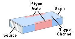
Fig.1.1 Diffusion JFET Construction
Fig. 1.1 shows the (theoretically) simplest form of construction for a Junction FET (JFET) using diffusion techniques. It uses a small slab of N type semiconductor into which are infused two P type areas to form the Gate. Current (electrons) flows through the device from source to drain along the N type silicon channel. As only one type of charge carrier (electrons) carry current in N channel JFETs, these transistors are also called "Unipolar" devices.
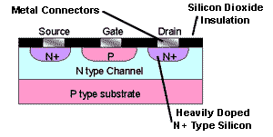
Watch it work with an interactive diagramFig. 1.2 JFET Planar Construction
Fig. 1.2 shows the cross section of a N channel planar Junction FET (JFET) The load current flows through the device from source to drain along a channel made of N type silicon. In the planar device the second part of the gate is formed by the P type substrate.
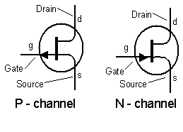
P channel JFETs are also available and the principle of operation is the same as the N channel type described here, but polarities of the voltages are of course reversed, and the charge carriers are holes.
Fig. 1.3 JFET Circuit symbols
No comments:
Post a Comment