http://en.wikipedia.org/wiki/Active_filter
Active filter
An active filter is a type of analog electronic filter that uses active components such as an amplifier. Amplifiers included in a filter design can be used to improve the performance and predictability of a filter,[1] while avoiding the need for inductors (which are typically expensive compared to other components). An amplifier prevents the load impedance of the following stage from affecting the characteristics of the filter. An active filter can have complex poles and zeros without using a bulky or expensive inductor. The shape of the response, the Q (quality factor), and the tuned frequency can often be set with inexpensive variable resistors. In some active filter circuits, one parameter can be adjusted without affecting the others. [1]
Using active elements has some limitations. Basic filter design equations neglect the finite bandwidth of amplifiers. Available active devices have limited bandwidth, so they are often impractical at high frequencies. Amplifiers consume power and inject noise into a system. Certain circuit topologies may be impractical if no DC path is provided for bias current to the amplifier elements. Power handling capability is limited by the amplifier stages.[2]

Active filter circuit configurations (electronic filter topology) include:
- Sallen and Key, and VCVS filters (low dependency on accuracy of the components)
- State variable and biquadratic filters
- Dual Amplifier Bandpass (DABP)
- Wien notch
- Multiple Feedback Filter
- Fliege (lowest component count for 2 opamp but with good controllability over frequency and type)
- Akerberg Mossberg (one of the topologies that offer complete and independent control over gain, frequency, and type)
Active filters can implement the same transfer functions as passive filters. Common transfer functions are:
- High-pass filter – attenuation of frequencies below their cut-off points.
- Low-pass filter – attenuation of frequencies above their cut-off points.
- Band-pass filter – attenuation of frequencies both above and below those they allow to pass.
- Notch filter – attenuation of certain frequencies while allowing all others to pass.
- Combinations are possible, such as notch and high-pass (in a rumble filter where most of the offending rumble comes from a particular frequency). Another example is an elliptic filter.
[edit]Design of active filters
To design filters, the specifications that need to be established include:
- The range of desired frequencies (the passband) together with the shape of the frequency response. This indicates the variety of filter (see above) and the center or corner frequencies.
- Input and output impedance requirements. These limit the circuit topologies available; for example, most, but not all active filter topologies provide a buffered (low impedance) output. However, remember that the internal output impedance of operational amplifiers, if used, may rise markedly at high frequencies and reduce the attenuation from that expected. Be aware that some high-pass filter topologies present the input with almost a short circuit to high frequencies.
- Dynamic range of the active elements. The amplifier should not saturate (run into the power supply rails) at expected input signals, nor should it be operated at such low amplitudes that noise dominates.
- The degree to which unwanted signals should be rejected.
- In the case of narrow-band bandpass filters, the Q determines the -3dB bandwidth but also the degree of rejection of frequencies far removed from the center frequency; if these two requirements are in conflict then a staggered-tuning bandpass filter may be needed.
- For notch filters, the degree to which unwanted signals at the notch frequency must be rejected determines the accuracy of the components, but not the Q, which is governed by desired steepness of the notch, i.e. the bandwidth around the notch before attenuation becomes small.
- For high-pass and low-pass (as well as band-pass filters far from the center frequency), the required rejection may determine the slope of attenuation needed, and thus the "order" of the filter. A second-order all-pole filter gives an ultimate slope of about 12 dB per octave (40dB/decade), but the slope close to the corner frequency is much less, sometimes necessitating a notch be added to the filter.
- The allowable "ripple" (variation from a flat response, in decibels) within the passband of high-pass and low-pass filters, along with the shape of the frequency response curve near the corner frequency, determine the damping factor (reciprocal of Q). This also affects the phase response, and the time response to a square-wave input. Several important response shapes (damping factors) have well-known names:
- Chebyshev filter – slight peaking/ripple in the passband before the corner; Q>0.7071 for 2nd-order filters
- Butterworth filter – flattest amplitude response; Q=0.7071 for 2nd-order filters
- Linkwitz–Riley filter – desirable properties for audio crossover applications; Q = 0.5 (critically damped)
- Paynter or transitional Thompson-Butterworth or "compromise" filter – faster fall-off than Bessel; Q=0.639 for 2nd-order filters
- Bessel filter – best time-delay, best overshoot response; Q=0.577 for 2nd-order filters
- Elliptic filter or Cauer filter – add a notch (or "zero") just outside the passband, to give a much greater slope in this region than the combination of order and damping factor without the notch.
Frequency Response and Active Filters
This document is an introduction to frequency response, and an introduction to active filters (filters using active amplifiers, like op amps). You might also want to read a similar document from National Semiconductor, A Basic Introduction to Filters - Active, Passive, and Switched-Capacitor.
Frequency Response -- Background
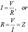
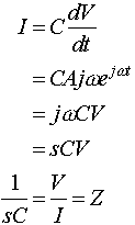
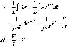
Up to now we have looked at the time-domain response of circuits. However it is often useful to look at the response of circuits in the frequency domain. In other words, you want to look at how circuits behave in response to sinusoidal inputs. This is important and useful for several reasons: 1) if the input to a linear circuit is a sinusoid, then the output will be a sinusoid at the same frequency, though its amplitude and phase may have changed, 2) any time domain signal can be decomposed via Fourier analysis into a series of sinusoids. Therefore if there is an easy way to analyze circuits with sinusoidal inputs, the results can be generalized to study the response to any input.To determine the response of a circuit to a sinusoidal signal as a function of frequency it is possible to generalize the concept of impedance to include capacitors and inductors. Consider a sinusoidal signal represented by a complex exponential:where j=(-1)1/2 (engineers use j instead of i, because i is used for current), w is frequency and t is time. It is a common shorthand to use "s" instead of "jw".Now let us look at the voltage-current relationships for resistors capacitors and inductors.For a resistor ohms law states:where we define the impedance, "Z", of a resistor as its resistance "R".For a capacitor we can also calculate the impedance assuming sinusoidal excitation starting from the current-voltage relationship:Note that for a capacitor the magnitude of the impedance, 1/wC, goes down with increasing frequency. This means that at very high frequencies the capacitor acts as an short circuit, and at low frequencies it acts as an open circuit. What is defined as a high, or low, frequency depends on the specific circuit in question.Likewise, for an inductor you can show that Z=sL.For an inductor, impedance goes up with frequency. It behaves as a short circuit at low frequencies, and an open circuit at high frequencies; the opposite of a capacitor. However inductors are not used often in electronic circuits due to their size, their susceptibility to parisitic effects (esp. magnetic fields), and because they do not behave as near to their ideal circuit elements as resistors and capacitors..
A Simple Low-Pass Circuit
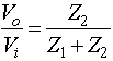
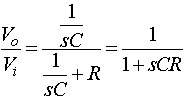
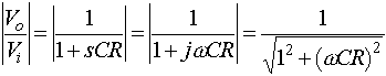
To see how complex impedances are used in practice consider the simple case of a voltage divider.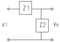 If Z1 is a resistor and Z2 is a capacitor thenGenerally we will be interested only in the magnitude of the response:Recall that the magnitude of a complex number is the square root of the sum of the squares of the real and imaginary parts. There are also phase shifts associated with the transfer function (or gain, Vo/Vi), thought we will generally ignore these.This is obviously a low pass filter (i.e., low frequency signals are passed and high frequency signals are blocked).. If w<<1/RC thenwCR<<1 and the magnitude of the gain is approximately unity, and the output equals the input. If w>>1/RC (wCR>>1 ) then the gain goes to zero, asdoes the output. At w=1/RC, called the break frequency (or cutoff frequency, or 3dB frequency, or half-power frequency, or bandwidth), the magnitude of the gain is 1/sqrt(2)@0.71. In this case (and all first order RC circuits) high frequency is defined as w>>1/RC; the capacitor acts as a short circuit and all the voltage is across the resistance. At low frequencies, w<<1/RC, the capacitor acts as an open circuit and there is no current (so the voltage across the resistor is near zero).If Z1 is an inductor and Z2 is a resistor another low pass structure results with a break frequency of R/L.
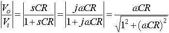
A Simple High-Pass Circuit
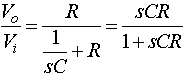
If Z1 is a capacitor and Z2 is a resistor we can repeat the calculation:andAt high frequencies, w>>1/RC, the capacitor acts as a short and the gain is 1 (the signal is passed). At low frequencies, w<<1/RC, the capacitor is an open and the output is zero (the signal is blocked). This is obviously a high pass structure and you can show that the break frequency is again 1/RC.
If Z1 is a resistor and Z2 is an inductor the resulting circuit is high pass with a break frequency of R/L.This concept of a complex impedance is extremely powerful and can be used when analyzing operational amplifier circuits, as you will soon see.
Active Filters
Low-Pass filters - the integrator reconsidered.
In the first lab with op-amps we considered the time response of the integrator circuit, but its frequency response can also be studied.
First Order Low Pass Filter with Op Amp
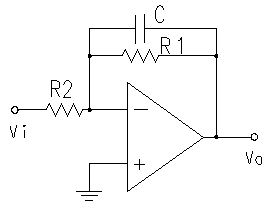
High-Pass filters - the differentiator reconsidered.
The circuit below is a modified differentiator, and acts as a high pass filter.
First Order High Pass Filter with Op Amp

Band-Pass circuits
Besides low-pass filters, other common types are high-pass (passes only high frequency signals), band-reject (blocks certain signals) and band-pass (rejects high and low frequencies, passing only signal areound some intermediate frequency).
The simplest band-pass filter can be made by combining the first order low pass and high pass filters that we just looked at.
This circuit will attenuate low frequencies (w<<1/R2C2) and high frequencies (w>>1/R1C1), but will pass intermediate frequencies with a gain of -R1/R2. However, this circuit cannot be used to make a filter with a very narrow band. To do that requires a more complex filter as discussed below.
Simple Band Pass Filter with Op Amp
High Q (Low Bandwidth) Bandpass Filters.
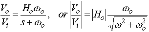
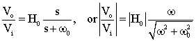
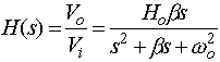
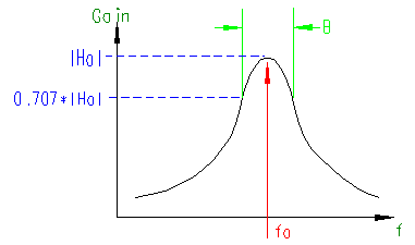
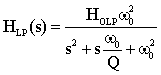
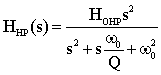
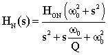
For a second-order band-pass filter the transfer function is given by

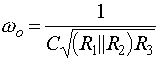
where wo is the center frequency, b is the bandwidth and Ho is the maximum amplitude of the filter. These quantities are shown on the diagram below. The quantities in parentheses are in radian frequencies, the other quantities are in Hertz (i.e. fo=wo/2p, B=b/2p). Looking at the equation above, or the figure, you can see that as w->0 and w->infinity that |H(s=jw)|->0. You can also easily show that at w=wo that |H(s=jwo)|=H0. Often you will see the equation above written in terms of the quality factor, Q, which can be defined in terms of the bandwidth, b, and center frequency, wo, as Q=wo/b. Thus the Q, or quality, of a filter goes up as it becomes narrower and its bandwidth decreases.If you derive the transfer function of the circuit shown below:
and the center frequency and bandwidth given by:
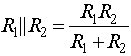
The notation R1||R2 denotes the parallel combination of R1 and R2,
Radian frequency Hertz
.


Switched Capacitor Filters
There is a special type of active filter, the switched capacitor filter, that takes advantage of integration to achieve very accurate filter characteristics that are electronically tuneable
http://www.swarthmore.edu/NatSci/echeeve1/Ref/FilterBkgrnd/SwitchedCap.html
Switched Capacitor Circuits
����������� In the last decade or so many active filters with resistors and capacitors have been replaced with a special kind of filter called a switched capacitor filter. The switched capacitor filter allows for very sophisticated, accurate, and tuneable analog circuits to be manufactured without using resistors.� This is useful for several reasons.� Chief among these is that resistors are hard to build on integrated circuits (they take up a lot of room), and the circuits can be made to depend on ratios of capacitor values (which can be set accurately), and not absolute values (which vary between manufacturing runs).
The Switched Capacitor Resistor
����������� To understand how switched capacitor circuits work, consider the circuit shown with a capacitor connected to two switches and two different voltages.�If S2 closes with S1 open, then S1 closes with switch S2 open, a charge (q is transferred from v2 to v1 with

If this switching process is repeated N times in a time (t, the amount of charge transferred per unit time is given by
Recognizing that the left hand side represents charge per unit time, or current, and the the number of cycles per unit time is the switching frequency (or clock frequency, fCLK) we can rewrite the equation as
Rearranging we get
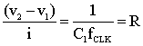 ,
,which states that the switched capacitor is equivalent to a resistor.� The value of this resistor decreases with increasing switching frequency or increasing capacitance, as either will increase the amount of charge transfered from v2 to v1 in a given time.
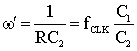
The Switched Capacitor Integrator
Now consider the integrator circuit.� You have shown (in a previous lab) that the input-output relationship for this circuit is given by (neglecting initial conditions):We can also write this with the "s" notation (assuming a sinusoidal input, Aest, s=jw)If you replaced the input resistor with a switched capacitor resistor, you would getThus, you can change the equivalent w' of the circuit by changing the clock frequency.� The value of w' can be set very precisely because it depends only on the ratio of C1 and C2, and not their absolute value.

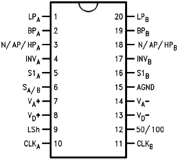
The LMF100 Switched Capacitor Filter
In this lab you will be using the MF100, or LMF100 (web page, datasheet, application note). This integrated circuit is a versatile circuit with four switched capacitor integrators, that can be connected as two second order filters or one fourth order filter.� With this chip you can choose w' to either be 1/50 or 1/100 of the clock frequency (this is given by the ratio C1/C2 in the discussion above),. By changing internal and external connections to the circuit you can obtain different filter types (lowpass, highpass, bandpass, notch (bandreject) or allpass).
Filter Type Transfer Function Low Pass High Pass Band Pass Notch (Band Reject)
- 50/100 - determines if the value of w' is wCLK/100, or wCLK/50.
- CLKA - is wCLK.
- INVA - the inverting input to the op-amp
- N/AP/HPA - an intermediate output, and the non-inverting input to the summer. Used for Notch, All Pass or High Pass output.
- BPA - another intermediate output, the output of the first integrator. Used for Band Pass output.
- LPA - the output of the second integrator. Used for Low Pass output.
- S1A - an inverting input to the summer.
- SAB - determins if the switch is to the left or to the right. That is, this pin determines if the second inverting input to the summer is ground (AGND), or the low pass output.
The two integrators are switched capacitor integrators. Their transfer functions are given by,where w' is wCLK/100, or wCLK/50, depending on the state of the 50/100 pin. Note that the integrator is non-inverting.A Typical Circuit.The diagram below shows one of the modes (mode 1) of operations (pages 13 through 20 of the datasheet).Let's analyze this circuit and try to derive the filter specifications as given in the datasheet, and given below.


No comments:
Post a Comment